TD1583PR Ver la hoja de datos (PDF) - Unspecified
Número de pieza
componentes Descripción
Fabricante
TD1583PR Datasheet PDF : 16 Pages
| |||
Techcode®
3A 380KHz 28V PWM Buck DC/DC Converter
Pin Configurations
DATASHEET
TD1583
Pin Description
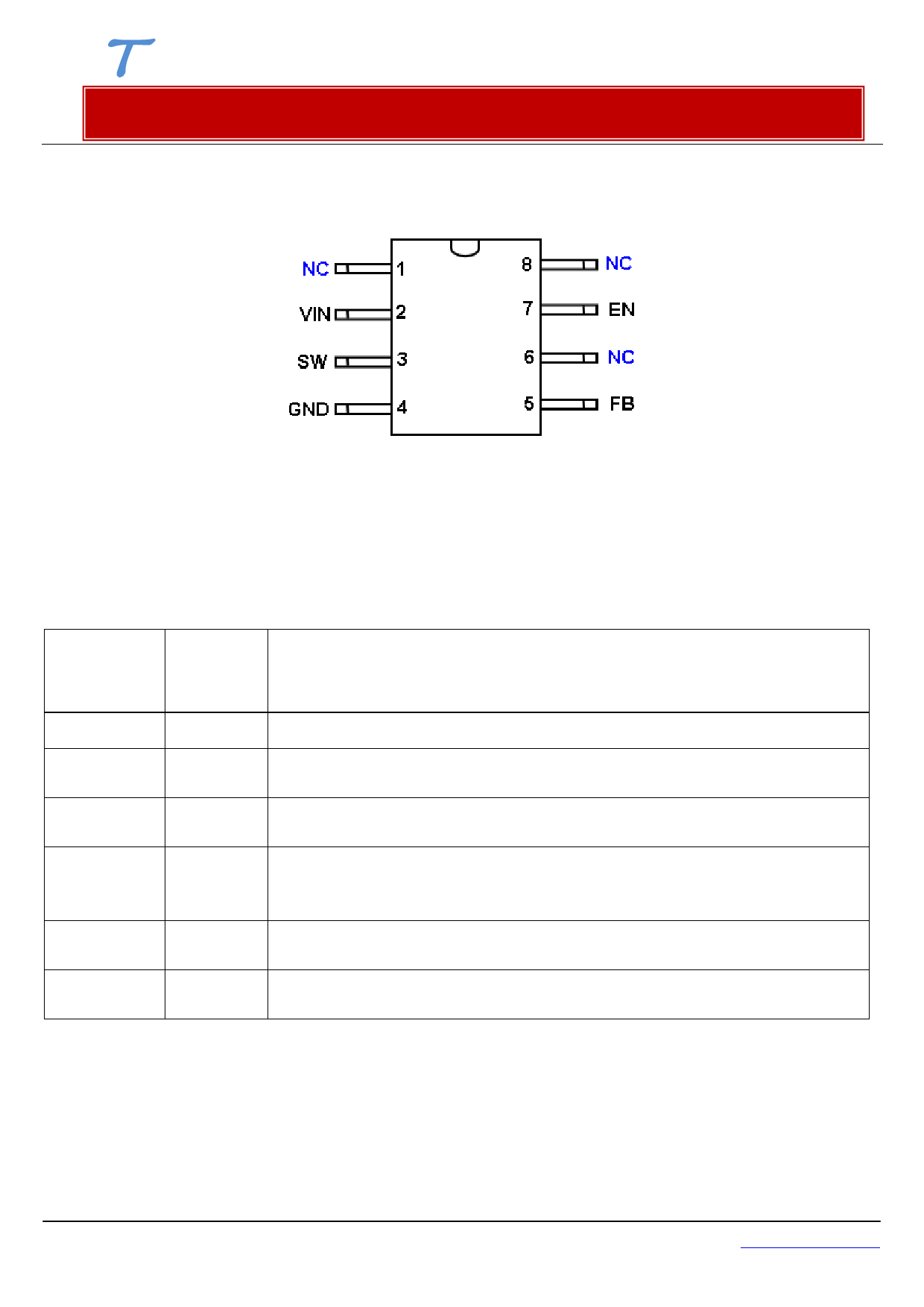
Figure 2 Pin Configuration of TD1583 (Top View)
Pin Number Pin Name Description
1,6, 8
2
3
4
5
7
NC
Vin
SW
GND
FB
EN
Not Connect.
Supply Voltage Input Pin. TD1583 operates from a 3.6V to 28V DC voltage.
Bypass Vin to GND with a suitably large capacitor to eliminate noise on the input.
Power Switch Output Pin. SW is the switch node that supplies power to the
output.
Ground Pin. Care must be taken in layout. This pin should be placed outside of
the Schottky Diode to output capacitor ground path to prevent switching current
spikes from inducing voltage noise into TD1583.
Feedback Pin. Through an external resistor divider network, FB senses the
output voltage and regulates it. The feedback threshold voltage is 1.222V.
Enable Pin. EN is a digital input that turns the regulator on or off .Drive EN pin
high to turn on the regulator, drive it low to turn it off.
December, 23, 2009.
Techcode Semiconductor Limited
2
www.techcodesemi.com
Share Link: 