BD6757KN Ver la hoja de datos (PDF) - ROHM Semiconductor
Número de pieza
componentes Descripción
Fabricante
BD6757KN
ROHM Semiconductor

BD6757KN Datasheet PDF : 16 Pages
| |||
BD6757KN, BD6889GU
Technical Note
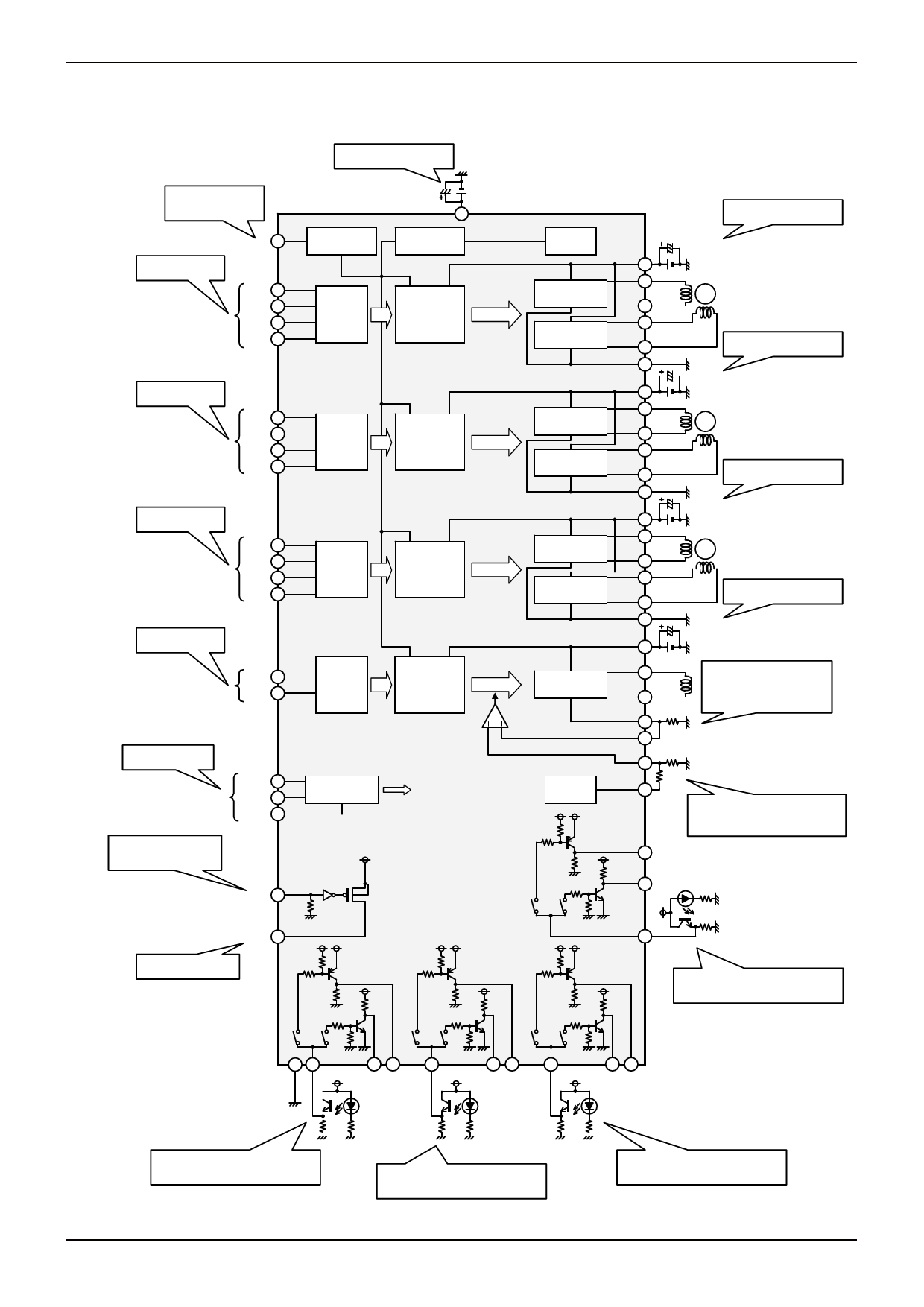
Bypass filter Capacitor for
power supply input. (p.14/16)
Power-saving (p.9/16)
H : Active
L : Standby
Motor control input
(p.9/16)
PS C7
IN1A E3
IN1B E4
IN2A F3
IN2B G3
Power Save
Logic12
1~100uF
VCC
D2
TSD & UVLO
Level Shift
&
Pre Driver
Motor control input
(p.9/16)
IN3A F6
IN3B F7
IN4A E6
IN4B E5
Motor control input
(p.9/16)
Motor control input
(p.9/16)
IN5A C6
IN5B D5
IN6A B3
IN6B B4
IN7A C4
IN7B D4
Logic34
Logic56
Logic7
Level Shift
&
Pre Driver
Level Shift
&
Pre Driver
Level Shift
&
Pre Driver
Selector for Digital
transistor (p.10/16)
REG Switch (p.10/16)
H : REG output ON
L : REG output OFF
DSEL1 E2
DSEL2 C3
DSW B2
DTR Selector
Digital
transistor SW
SW C2
VCC
Bypass filter Capacitor for
power supply input. (p.14/16)
BandGap
H bridge
Full ON
1~100uF
H5
VM1
H2 OUT1A
M
H3 OUT1B
H bridge
Full ON
H bridge
Full ON
H7
OUT2A
H6 OUT2B
H4 PGND1
1~100uF
D8
VM2
G8
OUT3A
M
F8 OUT3B
Bypass filter Capacitor for
power supply input. (p.14/16)
H bridge
Full ON
H bridge
Full ON
H bridge
Full ON
H bridge
Const. Current
VREF
VCC
VCC
B8
OUT4A
C8 OUT4B
E8 PGND2
1~100uF
Bypass filter Capacitor for
power supply input. (p.14/16)
A4
VM3
A7
OUT5A
M
A6 OUT5B
A2
OUT6A
A3 OUT6B
A5 PGND3
1~100uF
Bypass filter Capacitor for
power supply input. (p.14/16)
D1
VM4
C1
OUT7A
G1 OUT7B
RNF
E1
The output current is converted
to a voltage with the RNF
external resistor and transmitted
to the SENSE pin. (p.9/16)
Iout[A] = VLIM[V]÷RNF[Ω]
F1
0.1Ω~5.0Ω
SENSE
VLIM
F2
R2
R1
D3
VREF
When using the VREF voltage (0.9V)
resistance division value as VLIM input
value, select R1 and R2 values such that,
1kΩ≦R1+R2≦20kΩ (p.9/16)
VCC
B5 SO4P
B6 SO4N
SW
SW
REG
Power supply for photo
interrupter (p.10/16)
REG B7
VCC
VCC
VCC
VCC
VCC
VCC
VCC
VCC
C5 SI4
VCC
The sensor signal SI4, for lens position
detection, is reshaped and output to SO4x.
(p.10/16)
SW
SW
SW
SW
SW
SW
G2 F4
GND
SI1
G5
SO1N
REG
G4
SO1P
F5
SI2
G7
SO2N
REG
G6
SO2P
D6
SI3
E7
SO3N
REG
D7
SO3P
The sensor signal SI1, for lens position
detection, is reshaped and output to SO1x.
(p.10/16)
The sensor signal SI2, for lens position
detection, is reshaped and output to SO2x.
(p.10/16)
The sensor signal SI3, for lens position
detection, is reshaped and output to SO3x.
(p.10/16)
Fig.13 BD6889GU Application Circuit Diagram
www.rohm.com
© 2009 ROHM Co., Ltd. All rights reserved.
8/15
2009.06 - Rev.A
Share Link: