BD6757KN Ver la hoja de datos (PDF) - ROHM Semiconductor
Número de pieza
componentes Descripción
Fabricante
BD6757KN
ROHM Semiconductor

BD6757KN Datasheet PDF : 16 Pages
| |||
BD6757KN, BD6889GU
Technical Note
6) Digital transistor for photo-interrupter waveform shaping (BD6757KN and BD6889GU)
The BD6757KN, and BD6889GU build in two digital NPN transistor circuits, and eight digital NPN and PNP transistor
circuits for photo-interrupter waveform shaping, respectively. The sensor signal, for lens position detection, is reshaped
and output to the DSP. The input (SIx pin) is a dividing resistance type, and provided with NPN output (SOxN pin) pull-up
resistor and PNP output (SOxP pin) pull-down resistor. This is so that VCC, and GND voltage will be NPN output, and
PNP output, respectively, when the input is open. In the case of the BD6889GU, DSW, DSEL1, and DSEL2 pins can
control the switching of NPN and PNP transistor. The inputs are provided with input pull-down resistor. This is so that
GND voltage will be input, when these three pins are open. (See I/O Truth Table; P.12/16)
7) Voltage-regulator for photo-interrupter (BD6889GU)
The BD6889GU builds in voltage-regulator circuits for photo-interrupter. When High-level voltage is applied to SW pin,
the REG pin will be turned on. The input is provided with input pull-down resistor. This is so that REG pin will be turn off,
when the input is open.
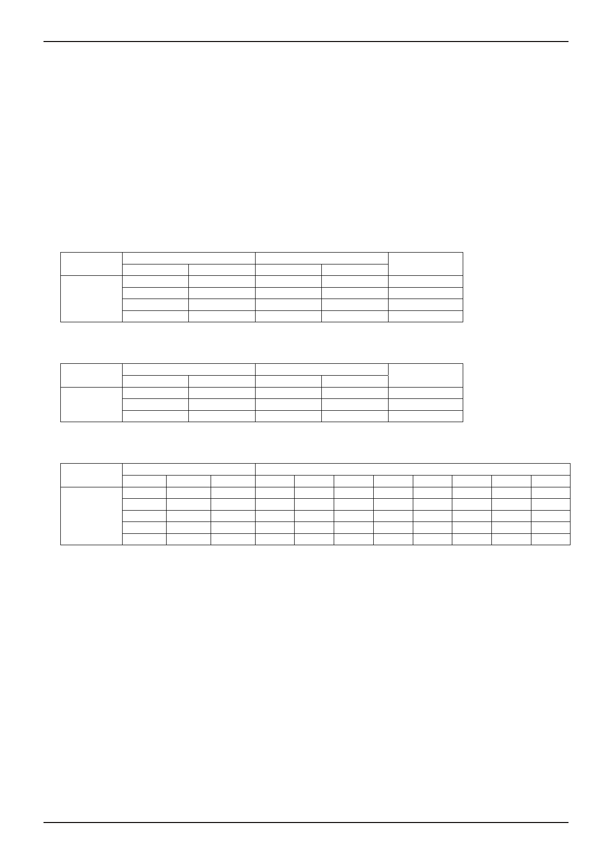
●I/O Truth Table
BD6757KN and BD6889GU Full-ON Driver ch1 to ch6 I/O Truth Table
Drive mode
INPUT
INxA
INxB
OUTPUT
OUTxA
OUTxB
L
L
Z
Z
IN/IN
H
L
L
H
H
L
L
H
H
H
L
L
L: Low, H: High, X: Don't care, Z: High impedance
At CW, current flows from OUTA to OUTB. At CCW, current flows from OUTB to OUTA.
Output mode
Standby
CW
CCW
Brake
BD6757KN and BD6889GU Linear Constant-Current Driver ch7 I/O Truth Table
Drive mode
INPUT
IN7A
IN7B
OUTPUT
OUT7A
OUT7B
L
X
Z
Z
EN/IN
H
L
H
L
H
H
L
H
L: Low, H: High, X: Don't care, Z: High impedance
At CW, current flows from OUTA to OUTB. At CCW, current flows from OUTB to OUTA.
Output mode
Standby
CW
CCW
BD6889GU Digital Transistor I/O Truth Table
INPUT
DSW DSEL1 DSEL2 PNP1 NPN1 PNP2
L
X
X
OFF OFF OFF
H
L
L
OFF
ON
OFF
Logic
H
L
H
OFF
ON
OFF
H
H
L
ON
OFF
ON
H
H
H
ON
OFF
ON
L: Low, H: High, X: Don’t care, OFF: GND (in the case of PNP), VCC (in the case of NPN)
PNPx output to SOxP terminal, NPNx output to SOxN terminal
OUTPUT
NPN2 PNP3
OFF OFF
ON
OFF
ON
ON
OFF OFF
OFF
ON
NPN3
OFF
ON
OFF
ON
OFF
PNP4
OFF
OFF
ON
OFF
ON
NPN4
OFF
ON
OFF
ON
OFF
www.rohm.com
© 2009 ROHM Co., Ltd. All rights reserved.
10/15
2009.06 - Rev.A
Share Link: