BD6369GUL Ver la hoja de datos (PDF) - ROHM Semiconductor
Número de pieza
componentes Descripción
Fabricante
BD6369GUL Datasheet PDF : 17 Pages
| |||
BD6883GUL,BH6453GUL,BD6886GUL,BD6369GUL
Technical Note
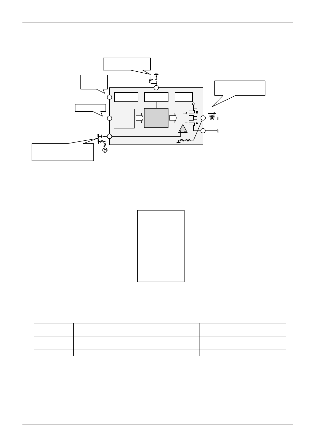
● Block Diagram, Application Circuit Diagram, Pin Arrangement, Pin Function Table
1) BD6883GUL Block Diagram, Application Circuit Diagram, Pin Arrangement, Pin Function Table
Bypass filter Capacitor for power
supply input. See. P.14/16.
Power-Saving
H: Active
L: Standby
0.1~10uF
VCC
1B
PS 1A Power Save
TSD & UVLO
Motor control input
IN 2A
Logic
Pre Driver
Setting for Constant-Voltage input terminal
In addition to the DC input, PWM signal drive
is also possible using filter components.
See. P.11/16
VLIM
2B
BandGap
×2
VCC
ISOURCE
1C
OUT
GND
2C
0.5ch Constant-Voltage output pins.
Output H voltage.
OUT[V]=2×VLIM[V]
Fig.19 BD6883GUL Block Diagram, Application Circuit Diagram
1
2
A PS
IN
B VCC
VLIM
C OUT
GND
Fig.20 BD6883GUL Pin Arrangement (Top View)
BD6883GUL Pin Function Table
No.
Pin
Name
Function
1A
PS Power-saving pin
2A
IN
Control input pin
1B
VCC Power supply pin
No.
Pin
Name
Function
2B VLIM Output high-level voltage setting pin
1C OUT Half-bridge output pin
2C GND Ground pin
www.rohm.com
© 2012 ROHM Co., Ltd. All rights reserved.
7/16
2012.03 - Rev.A
Share Link: 