CXA3235 Ver la hoja de datos (PDF) - Sony Semiconductor
Número de pieza
componentes Descripción
Fabricante
CXA3235 Datasheet PDF : 23 Pages
| |||
CXA3235/3236N
Description of PLL Block
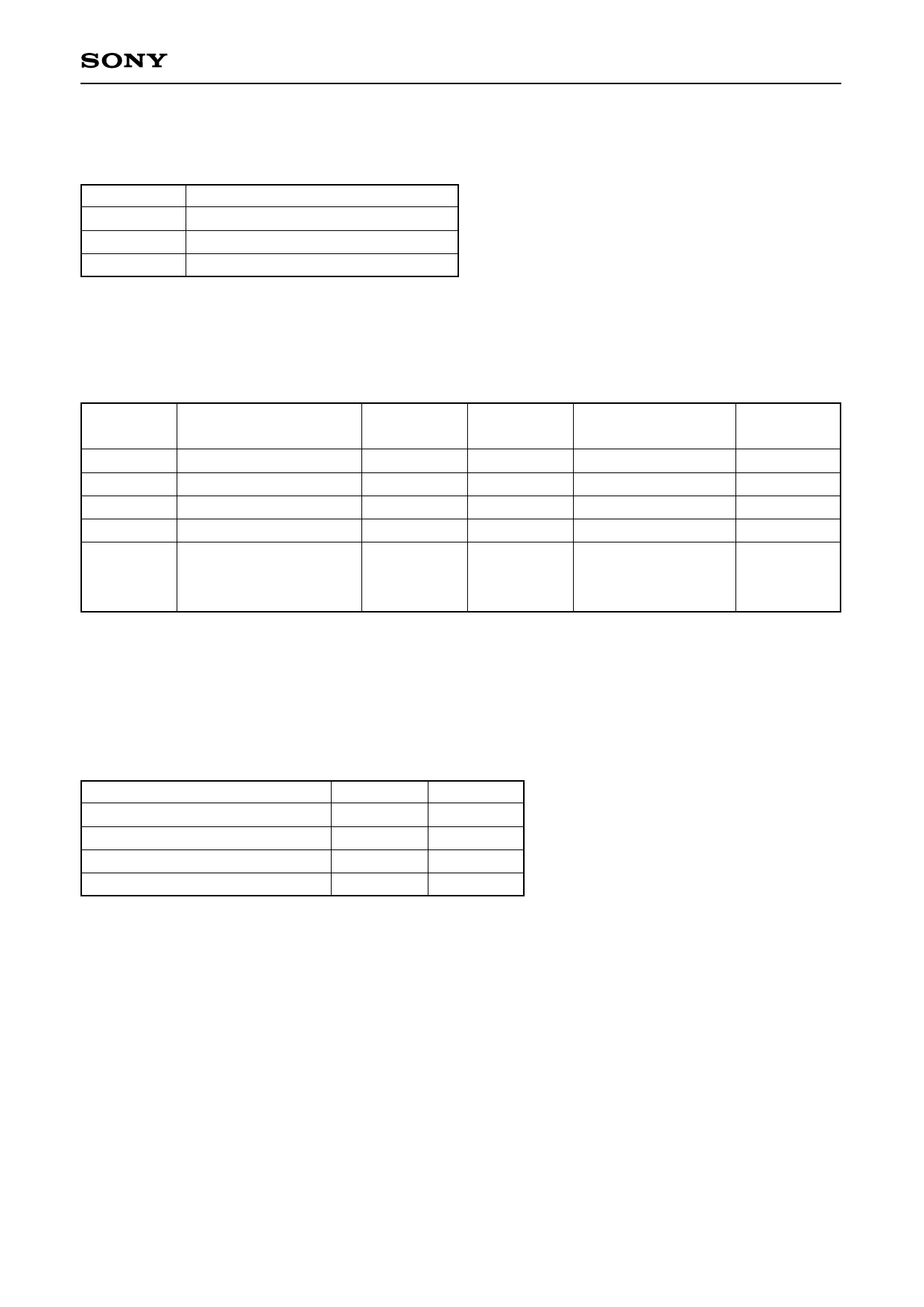
The PLL on this IC supports the I2C bus control format. The control pins are as shown in the table below.
Symbol
ADSW
SCL
SDA
Description
Address selection
SCL input
SDA I/O
1) Mode Setting Method
The modes for each frequency step are set according to the MS pin voltage.
Mode
B-0
B-1
B-2
B-3
B-4
MS pin voltage
0 to 0.15 VCC
OPEN
0.45 VCC to 0.55 VCC
0.65 VCC to 0.75 VCC
0.85 VCC to VCC
Main
divider
15 bit
14 bit
15 bit
15 bit
15 bit
Reference
divider
1024
512
640
512
512/
640/
1024
Reference frequency
3.90625 kHz
7.8125 kHz
6.25 kHz
7.8125 kHz
7.8125 kHz/
6.25 kHz/
3.90625 kHz
∗ Frequency step is for when X’tal OSC = 4 MHz.
Frequency
step∗
31.25 kHz
62.5 kHz
50 kHz
62.5 kHz
62.5 kHz/
50 kHz/
31.25 kHz
2) Address Setting
The responding address can be changed according to the ADSW pin voltage, so that multiple PLL can
exist within one system.
Address
ADSW pin voltage
0 to 0.1 VCC
OPEN or 0.2 VCC to 0.3 VCC
0.4 VCC to 0.6 VCC
0.9 VCC to VCC
MA1
0
0
1
1
MA0
0
1
0
1
—11—
Share Link: 