STK433-090-E Ver la hoja de datos (PDF) - SANYO -> Panasonic
Número de pieza
componentes Descripción
Fabricante
STK433-090-E Datasheet PDF : 11 Pages
| |||
STK433-090-E
[Example]
When the IC supply voltage, VCC, is ±33V and RL is 6Ω, the total power dissipation, Pd, within the hybrid IC, will
be a maximum of 75W at 1kHz for a continuous sine wave signal according to the Pd-PO characteristics.
For the music signals normally handled by audio amplifiers, a value of 1/8PO max is generally used for Pd as an
estimate of the power dissipation based on the type of continuous signal. (Note that the factor used may differ
depending on the safety standard used.)
This is:
Pd ≈ 59.0W
(when 1/8PO max. = 10W, PO max. = 80W).
The number of power transistors in audio amplifier block of these hybrid ICs, N, is 4, and the thermal resistance per
transistor, θj-c, is 2.1°C/W. Therefore, the required heat sink thermal resistance for a guaranteed ambient temperature,
Ta, of 50°C will be as follows.
From formula (1)'
θc-a < (125 − 50)/59.0
< 1.27
From formula (2)'
θc-a < (150 − 50)/59.0 − 2.1/4
< 1.17
Therefore, the value of 1.17°C/W, which satisfies both of these formulae, is the required thermal resistance of the heat
sink.
Note that this thermal design example assumes the use of a constant-voltage power supply, and is therefore not a
verified design for any particular user’s end product.
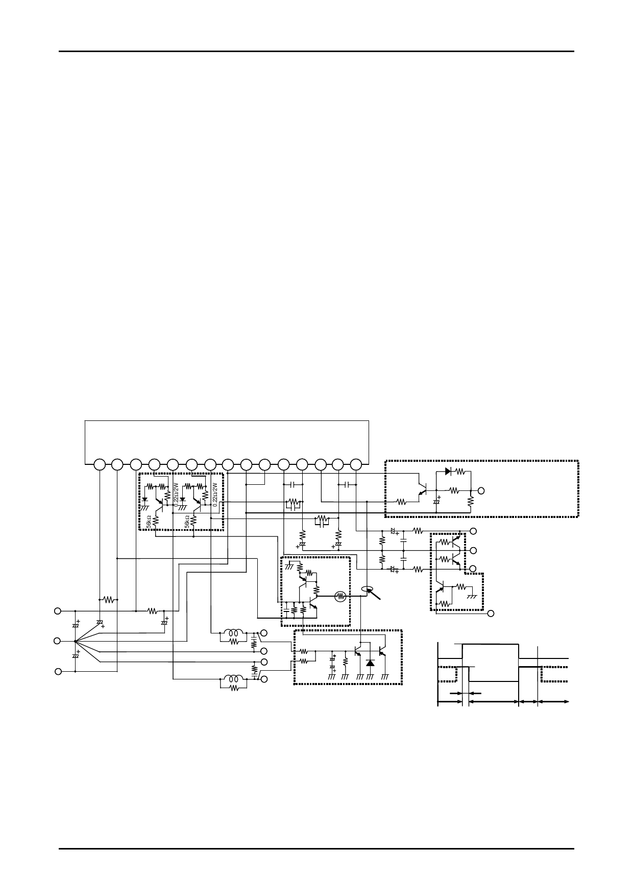
STK433-100 Series Standby Control, Mute Control, Load-short Protection & DC
offset Protection application
+VCC
GND
-VCC
STK433-100 series
Ch1 Ch1 Ch2 Ch2
Ch1 Ch1
Ch2 Ch2
-PRE -VCC +VCC OUT OUT OUT OUT +PRE SUB GND IN NF ST-BY NF IN
1 2 3 4 5 6 7 8 9 10 11 12 13 14 15
56kΩ6.8kΩ 56kΩ 6.8kΩ
(*1) The voltage applied to the Stand-by pin (#13) must not exceed the
maximum rated value (VST max).
(*1)
13kΩ
1kΩ
33kΩ
33μF
2kΩ
/10V
Stand-by Control (ex)
H: Operation Mode (+5V)
L: Stand-by Mode (0V)
Load short
protection
circuit
22kΩ
56kΩ
Latch up
circuit
1kΩ
0.1μF
R1
V1
(*1)
10kΩ 100kΩ
Ch2 OUT
82kΩ
GND
GND
22μF
100
82kΩ 22μF
kΩ
Ch1 OUT
DC offset protection
Ch2 IN
10kΩ
GND
10kΩ
10kΩ
Ch1 IN
2.2kΩ
Mute Control
H: Single Mute
L: Normal
+5V
Standby
Control
Mute
Control
ST-BY
+5V
MUTE
PLAY
MUTE ST-BY
No. A1248-8/11
Share Link: 