STK433-090-E Ver la hoja de datos (PDF) - SANYO -> Panasonic
Número de pieza
componentes Descripción
Fabricante
STK433-090-E Datasheet PDF : 11 Pages
| |||
STK433-090-E
Specifications
Absolute maximum ratings at Ta=25°C (excluding rated temperature items), Tc=25°C unless otherwise specified
Parameter
Maximum quiescent supply voltage 0
Maximum supply voltage 1
Minimum operating supply voltage
Maximum operating flow-in current (pin 13) *7
Thermal resistance
Junction temperature
IC substrate operating temperature
Storage temperature
Allowable load shorted time
*4
Symbol
VCC max (0)
VCC max (1)
VCC min
IST OFF max
θj-c
Tj max
Tc max
Tstg
ts
When no signal
RL≥6Ω
Conditions
Per power transistor
Both the Tj max and Tc max conditions must be met.
VCC=±33V, RL=6Ω, f=50Hz, PO=50W,
1-channel active
Ratings
±54
±47
±10
0.6
2.1
150
125
-30 to +125
0.3
Unit
V
V
V
mA
°C/W
°C
°C
°C
s
Operating Characteristics at Tc=25°C, RL=6Ω, Rg=600Ω, VG=30dB, non-inductive load RL, unless otherwise
specified
Conditions *2
Ratings
Parameter
Symbol
VCC
f
PO THD
(V)
(Hz)
(W) (%)
unit
min
typ
max
Output power
*1 PO (1)
±33 20 to 20k
0.4
PO (2)
±33
1k
10
47
50
W
80
Total harmonic distortion *1
THD (1)
THD (2)
±33 20 to 20k
5.0
±33
1k
VG=30dB
0.4
%
0.01
Frequency characteristics *1 fL, fH
±33
1.0
+0 -3dB
20 to 50k
Hz
Input impedance
ri
±33
1k
1.0
55
kΩ
Output noise voltage
*3 VNO
±39
Rg=2.2kΩ
1.0 mVrms
Quiescent current
ICCO
±39
No loading
20
45
80 mA
Output neutral voltage
VN
±39
-70
0
+70 mV
Current flowing into pin13 in
IST ON
±33
standby mode
*7
Current flowing into pin13 in
IST OFF
±33
operating mode
*7
Voltage at pin13: 5V,
Current limiting
resistance R1: 13kΩ
0.25
0 mA
0.6 mA
[Remarks]
*1: For 1-channel operation
*2: Unless otherwise specified, use a constant-voltage power supply to supply power when inspections are carried out.
*3: The output noise voltage values shown are peak values read with a VTVM. However, an AC stabilized (50Hz)
power supply should be used to minimize the influence of AC primary side flicker noise on the reading.
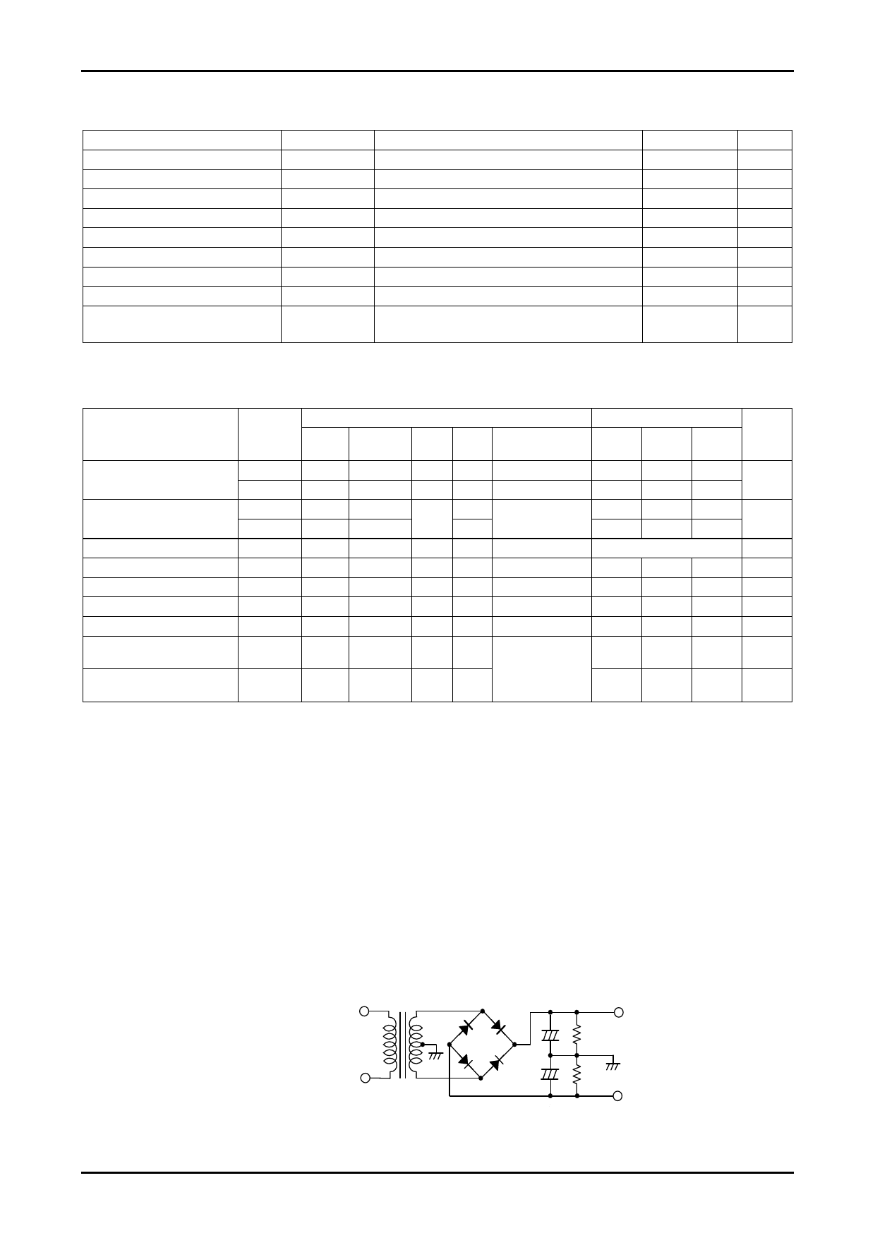
*4: Use the designated transformer power supply circuit shown in the figure below for the measurement of allowable
load shorted time and output noise voltage.
*5: The –Pre VCC (pin 1) line must be at the lowest level under any circumstances.
*6: Thermal design must be implemented based on the conditions under which the customer’s end products are
expected to operate on the market.
*7: Be sure to use the current limiting resistor to prevent the current flowing into the standby pin (pin13) never exceeds
the maximum rated value in operating mode.
The circuit is turned on by applying VBE (approximately 0.6V) or higher voltage to the standby pin (pin13).
*8: A thermoplastic adhesive resin is used for this hybrid IC.
Designated transformer power supply
(MG-200 equivalent)
DBA40C
10000μF
+
500Ω
+VCC
+
500Ω
10000μF
-VCC
No. A1248-2/11
Share Link: 