CXD2587 Ver la hoja de datos (PDF) - Sony Semiconductor
Número de pieza
componentes Descripción
Fabricante
CXD2587 Datasheet PDF : 106 Pages
| |||
CXD2587Q
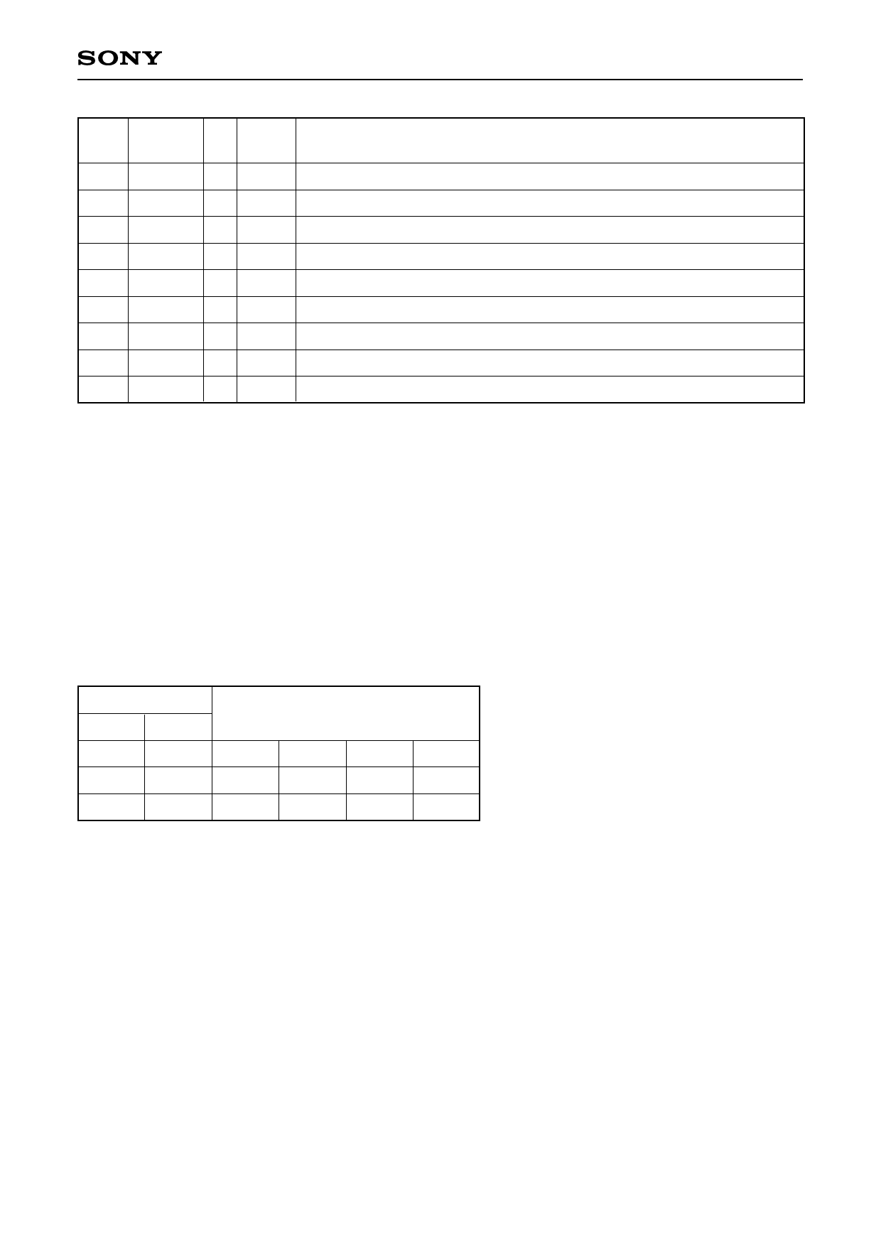
Pin
No.
Symbol
I/O
Output
values
Description
72 LOUT1 O
L ch LINE output.
73 AVSS1 — — Analog GND.
74 AVSS2 — — Analog GND.
75 LOUT2 O
R ch LINE output.
76 AIN2
I
R ch operational amplifier output.
77 AOUT2 O
R ch analog output.
78 AVDD2 — — Analog power supply.
79 RMUT O 1, 0 R ch zero detection flag.
80 LMUT
O 1, 0 L ch zero detection flag.
Notes) • PCMD is a MSB first, two's complement output.
• GTOP is used to monitor the frame sync protection status. (High: sync protection window released.)
• XUGF is the frame sync obtained from the EFM signal, and is negative pulse. It is the signal before
sync protection.
• XPCK is the inverse of the EFM PLL clock. The PLL is designed so that the falling edge and the
EFM signal transition point coincide.
• The GFS signal goes high when the frame sync and the insertion timing match.
• RFCK is derived from the crystal accuracy, and has a cycle of 136µs.
• C2PO represents the data error status.
• XROF is generated when the 16K RAM exceeds the ±4F jitter margin.
Monitor Pin Output Combinations
Command bit
MTSL1 MTSL0
Output data
0
0
XUGF XPCK GFS
0
1
MNT1 MNT0 MNT3
1
0
RFCK XPCK XROF
C2PO
C2PO
GTOP
–6–
Share Link: 