CXD2587 Ver la hoja de datos (PDF) - Sony Semiconductor
Número de pieza
componentes Descripción
Fabricante
CXD2587 Datasheet PDF : 106 Pages
| |||
CXD2587Q
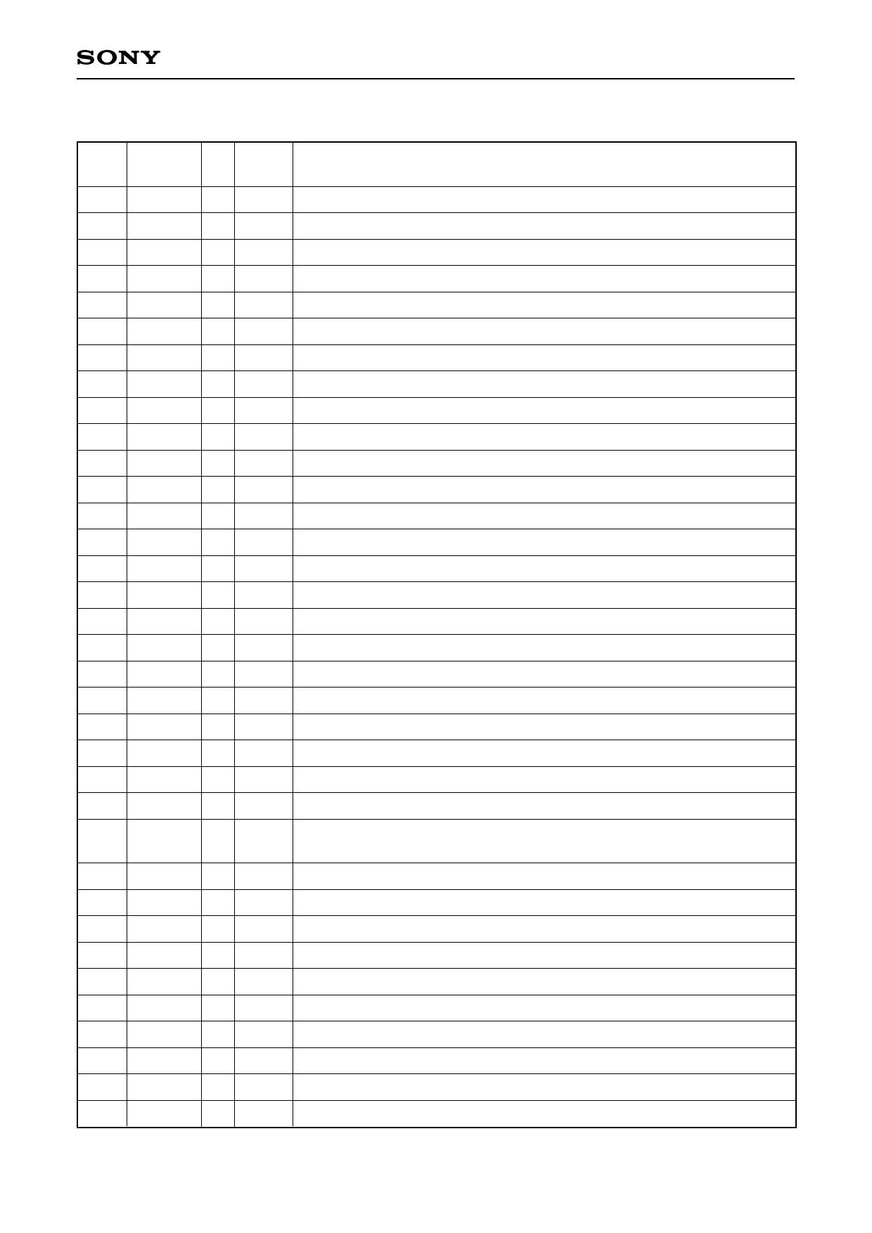
Pin Description
Pin
No.
Symbol
I/O
Output
values
Description
1 SQSO O 1, 0 Sub Q 80-bit, PCM peak and level data outputs. CD TEXT data output.
2 SQCK
I
SQSO readout clock input.
3 XRST
I
System reset. Reset when low.
4 SYSM
I
Mute input. Muted when high.
5 DATA
I
Serial data input from CPU.
6 XLAT
I
Latch input from CPU. Serial data is latched at the falling edge.
7 CLOK
I
Serial data transfer clock input from CPU.
8 SENS
O 1, 0 SENS output to CPU.
9 SCLK
I
SENS serial data readout clock input.
10 VDD
— — Digital power supply.
11 ATSK I/O 1, 0 Anti-shock input/output.
12 SPOA
I
Microcomputer extension interface (input A)
13 SPOB
I
Microcomputer extension interface (input B)
14 XLON
O 1, 0 Microcomputer extension interface (output)
15 WFCK O 1, 0 WFCK output.
16 XUGF O 1, 0 XUGF output. MINT1 or RFCK is output by switching with the command.
17 XPCK
O 1, 0 XPCK output. MNT0 is output by switching with the command.
18 GFS
O 1, 0 GFS output. MNT3 or XROF is output by switching with the command.
19 C2PO
O 1, 0 C2PO output. GTOP is output by switching with the command.
20 SCOR O 1, 0 Outputs a high signal when either subcode sync S0 or S1 is detected.
21 COUT I/O 1, 0 Track count signal input/output.
22 MIRR I/O 1, 0 Mirror signal input/output.
23 DFCT I/O 1, 0 Defect signal input/output.
24 FOK
I/O 1, 0 Focus OK signal input/output.
25 LOCK
I/O
1, 0
GFS is sampled at 460Hz; when GFS is high, this pin outputs a high signal. If GFS
is low eight consecutive samples, this pin outputs low. Or input when LKIN = 1.
26 MDP
O 1, Z, 0 Spindle motor servo control output.
27 SSTP
I
Disc innermost track detection signal input.
28 SFDR
O 1, 0 Sled drive output.
29 SRDR O 1, 0 Sled drive output.
30 TFDR
O 1, 0 Tracking drive output.
31 TRDR O 1, 0 Tracking drive output.
32 FFDR
O 1, 0 Focus drive output.
33 FRDR O 1, 0 Focus drive output.
34 VSS
— — Digital GND.
35 TEST
I
Test pin. Normally, GND.
–4–
Share Link: 