SMCJLCE80A Ver la hoja de datos (PDF) - Microsemi Corporation
Número de pieza
componentes Descripción
Fabricante
SMCJLCE80A
Microsemi Corporation

SMCJLCE80A Datasheet PDF : 4 Pages
| |||
SCOTTSDALE DIVISION
SMCGLCE6.5 thru SMCGLCE170A, e3
SMCJLCE6.5 thru SMCJLCE170A, e3
1500 WATT LOW CAPACITANCE
SURFACE MOUNT TRANSIENT
VOLTAGE SUPPRESSOR
DESCRIPTION
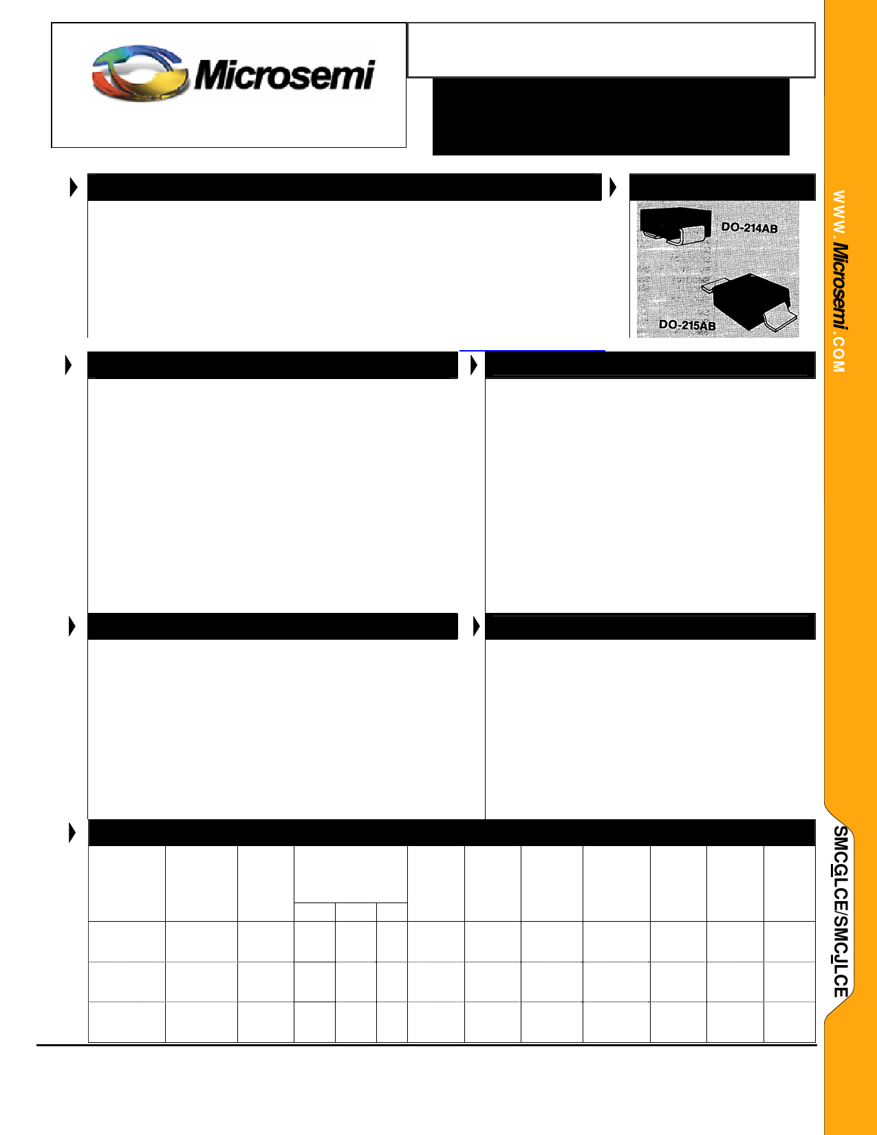
APPEARANCE
This surface mount Transient Voltage Suppressor (TVS) product family includes a
rectifier diode element in series and opposite direction to achieve low capacitance
below 100 pF. They are also available as RoHS Compliant with an e3 suffix. The low
TVS capacitance may be used for protecting higher frequency applications in inductive
switching environments or electrical systems involving secondary lightning effects per
IEC61000-4-5 as well as RTCA/DO-160D or ARINC 429 for airborne avionics. They
also protect from ESD and EFT per IEC61000-4-2 and IEC61000-4-4. If bipolar
transient capability is required, two of these low capacitance TVS devices may be used
in parallel and opposite directions (anti-parallel) for complete ac protection (Figure 6).
IMPORTANT: For the most current data, consult MICROSEMI’s website: http://www.microsemi.com
FEATURES
APPLICATIONS / BENEFITS
• Available in standoff voltage range of 6.5 to 200 V
• Low capacitance of 100 pF or less
• Molding compound flammability rating: UL94V-O
• Two different terminations available in C-bend (modified J-
Bend with DO-214AB) or Gull-wing (DO-215AB)
• Options for screening in accordance with MIL-PRF-19500
for JAN, JANTX, JANTXV, and JANS are available by
adding MQ, MX, MV, or MSP prefixes respectively to part
numbers
• Optional 100% screening for avionics grade is available by
adding MA prefix to part number for 100% temperature
cycle –55ºC to 125ºC (10X) as well as surge (3X) and 24
hours HTRB with post test VBR & IR
• RoHS Compliant devices available by adding an “e3” suffix
• 1500 Watts of Peak Pulse Power at 10/1000 μs
• Protection for aircraft fast data rate lines per select
level waveforms in RTCA/DO-160D & ARINC 429
• Low capacitance for high speed data line
interfaces
• IEC61000-4-2 ESD 15 kV (air), 8 kV (contact)
• IEC61000-4-5 (Lightning) as further detailed in
LCE6.5 thru LCE170A data sheet
• T1/E1 Line Cards
• Base Stations
• WAN Interfaces
• XDSL Interfaces
• CSU/DSU Equipment
MAXIMUM RATINGS
• 1500 Watts of Peak Pulse Power dissipation at 25oC with
repetition rate of 0.01% or less*
• Clamping Factor: 1.4 @ Full Rated power
1.30 @ 50% Rated power
• tclamping (0 volts to V(BR) min): Less than 5x10⁻⁹ seconds
• Operating and Storage temperatures: -65 to +150oC
• Steady State power dissipation: 5.0W @ TL = 50oC
• THERMAL RESISTANCE: 20oC/W (typical junction to
lead (tab) at mounting plane
* When pulse testing, do not pulse in opposite direction
(see “Schematic Applications” section herein and
Figures 5 & 6 for further protection in both directions)
ELECTRICAL CHARACTERISTICS @ 25oC
MICROSEMI
Part Number
Gull-Wing
“G”
Bend Lead
SMCGLCE6.5
SMCGLCE6.5A
SMCGLCE7.0
SMCGLCE7.0A
SMCGLCE7.5
SMCGLCE7.5A
SMCGLCE8.0
SMCGLCE8.0A
SMCGLCE8.5
SMCGLCE8.5A
SMCGLCE9.0
SMCGLCE9.0A
MICROSEMI
Part Number
Modified
“J”
Bend Lead
SMCJLCE6.5
SMCJLCE6.5A
SMCJLCE7.0
SMCJLCE7.0A
SMCJLCE7.5
SMCJLCE7.5A
SMCJLCE8.0
SMCJLCE8.0A
SMCJLCE8.5
SMCJLCE8.5A
SMCJLCE9.0
SMCJLCE9.0A
Reverse
Stand-Off
Voltage
VWM
Volts
6.5
6.5
7.0
7.0
7.5
7.5
8.0
8.0
8.5
8.5
9.0
9.0
Breakdown Voltage
VBR @ I(BR)
Volts
MIN
MAX mA
7.22
8.82
10
7.22
7.98
10
7.78
9.51
10
7.78
8.60
10
8.33
10.2
10
8.33
9.21
10
8.89
10.9
1
8.89
9.83
1
9.44 11.5
1
9.44 10.4
1
10.0 12.2
1
10.0 11.1
1
Maximum
Reverse
Leakage
@VWM
ID
μA
1000
1000
500
500
250
250
100
100
50
50
10
10
MECHANICAL AND PACKAGING
• CASE: Molded, surface mountable
• TERMINALS: Gull-wing or C-bend (modified J-
bend) tin-lead or RoHS compliant annealed
matte-tin plating solderable per MIL-STD-750,
method 2026
• POLARITY: Cathode indicated by band
• MARKING: Part number without prefix (e.g.
LCE6.5A, LCE6.5Ae3, LCE33, LCE33Ae3, etc.
• TAPE & REEL option: Standard per EIA-481-B
with 16 mm tape, 750 per 7 inch reel or 2500 per
13 inch reel (add “TR” suffix to part number)
Maximum
Clamping
Voltage
@IPP
VC
Volts
12.3
11.2
13.3
12.0
14.3
12.9
15.0
13.6
15.9
14.4
16.9
15.4
Maximum
Peak Pulse
Current IPP
@10/1000
Amps
100
100
100
100
100
100
100
100
94
100
89
97
Maximum
Capacitance
@ 0 Volts,
f = 1 MHz
pF
75
75
75
75
100
100
100
100
100
100
100
100
VWIBB
Working
Inverse
Blocking
Voltage
Volts
75
75
75
75
75
75
75
75
75
75
75
75
IIB
Inverse
Blocking
Leakage
Current
mA
1
1
1
1
1
1
1
1
1
1
1
1
VPIB
Peak
Inverse
Blocking
Voltage
Volts
100
100
100
100
100
100
100
100
100
100
100
100
Copyright © 2005
6-06-2005 REV D
Microsemi
Scottsdale Division
8700 E. Thomas Rd. PO Box 1390, Scottsdale, AZ 85252 USA, (480) 941-6300, Fax: (480) 947-1503
Page 1
Share Link: