03N60Z Ver la hoja de datos (PDF) - ON Semiconductor
Número de pieza
componentes Descripción
Fabricante
03N60Z Datasheet PDF : 10 Pages
| |||
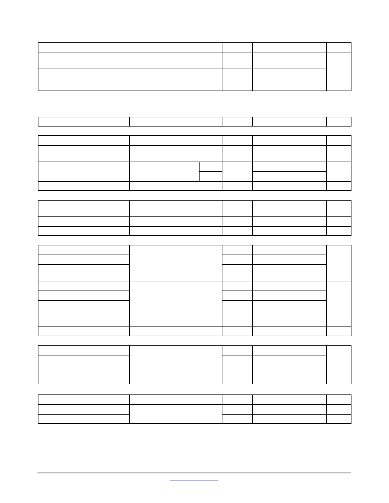
NDF03N60Z, NDD03N60Z
THERMAL RESISTANCE
Junction−to−Case (Drain)
Parameter
NDF03N60Z
NDD03N60Z
Symbol
RqJC
Value
4.7
2.0
Unit
°C/W
Junction−to−Ambient Steady State
(Note 3) NDF03N60Z
RqJA
51
(Note 4) NDD03N60Z
40
(Note 3) NDD03N60Z−1
80
3. Insertion mounted
4. Surface mounted on FR4 board using 1″ sq. pad size, (Cu area = 1.127 in sq [2 oz] including traces).
ELECTRICAL CHARACTERISTICS (TJ = 25°C unless otherwise noted)
Characteristic
Test Conditions
Symbol
Min
Typ
Max
Unit
OFF CHARACTERISTICS
Drain−to−Source Breakdown Voltage
Breakdown Voltage Temperature Co-
efficient
VGS = 0 V, ID = 1 mA
Reference to 25°C,
ID = 1 mA
BVDSS
600
DBVDSS/
0.6
DTJ
V
V/°C
Drain−to−Source Leakage Current
VDS = 600 V, VGS = 0 V
25°C
150°C
IDSS
1
mA
50
Gate−to−Source Forward Leakage
VGS = ±20 V
IGSS
±10
mA
ON CHARACTERISTICS (Note 5)
Static Drain−to−Source
On−Resistance
VGS = 10 V, ID = 1.2 A
RDS(on)
3.3
3.6
W
Gate Threshold Voltage
Forward Transconductance
DYNAMIC CHARACTERISTICS
Input Capacitance (Note 6)
Output Capacitance (Note 6)
Reverse Transfer Capacitance
(Note 6)
VDS = VGS, ID = 50 mA
VDS = 15 V, ID = 1.5 A
VDS = 25 V, VGS = 0 V,
f = 1.0 MHz
VGS(th)
3.0
3.9
4.5
V
gFS
2.0
S
Ciss
248
312
372
pF
Coss
30
39
50
Crss
4
8
12
Total Gate Charge (Note 6)
Gate−to−Source Charge (Note 6)
Gate−to−Drain (“Miller”) Charge
(Note 6)
VDD = 300 V, ID = 3.0 A,
VGS = 10 V
Qg
6
12
18
nC
Qgs
1.5
2.5
4
Qgd
3
6.1
9
Plateau Voltage
VGP
6.4
V
Gate Resistance
Rg
6.0
W
RESISTIVE SWITCHING CHARACTERISTICS
Turn−On Delay Time
td(on)
9
ns
Rise Time
Turn−Off Delay Time
VDD = 300 V, ID = 3.0 A,
tr
8
VGS = 10 V, RG = 5 W
td(off)
16
Fall Time
tf
10
SOURCE−DRAIN DIODE CHARACTERISTICS (TC = 25°C unless otherwise noted)
Diode Forward Voltage
IS = 3.0 A, VGS = 0 V
VSD
1.6
V
Reverse Recovery Time
Reverse Recovery Charge
VGS = 0 V, VDD = 30 V
trr
IS = 3.0 A, di/dt = 100 A/ms
Qrr
265
ns
0.9
mC
Product parametric performance is indicated in the Electrical Characteristics for the listed test conditions, unless otherwise noted. Product
performance may not be indicated by the Electrical Characteristics if operated under different conditions.
5. Pulse Width ≤ 380 ms, Duty Cycle ≤ 2%.
6. Guaranteed by design.
www.onsemi.com
2
Share Link: 