TRW Ver la hoja de datos (PDF) - Unspecified
Número de pieza
componentes Descripción
Fabricante
TRW Datasheet PDF : 59 Pages
| |||
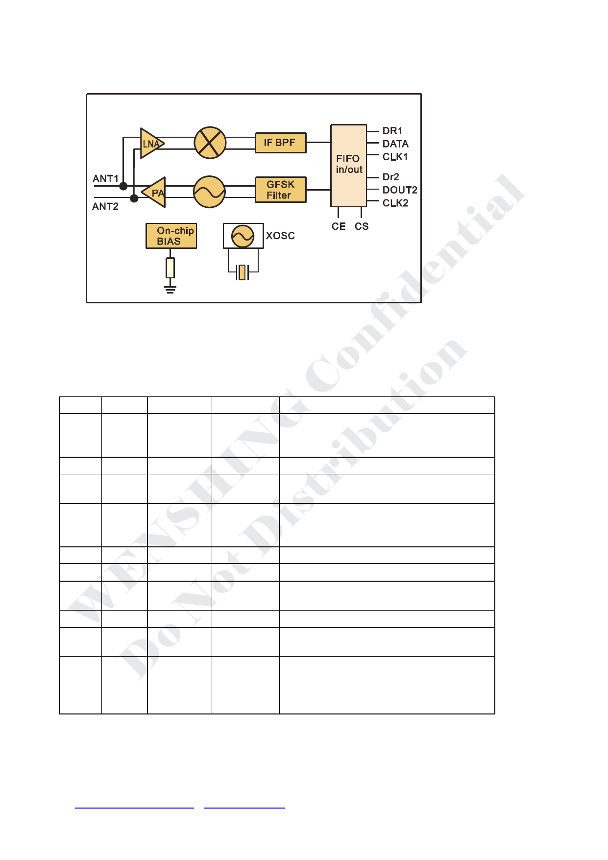
2 Block Diagram
This block diagram details the whole structure of this module which allows user to adopt two
channels simultaneously without adding any extra components except micro-controller. We shall
have reference schematic how this module works with micro-controller in the subsequence.
3 Pin Function
Pin Name Category I/O
Description
1
CLK1
Digital Input/Output For channel 1 clock
TX: Clock input
RX: Clock input/output
2
CS
Digital
Input
Chip selection activates Configuration Mode
3
CLK2
Digital Input/Output For channel 2 clock
Rx: Clock input/output
4
CE
Digital
5
GND
Power
Input
Chip Enable to active RX / TX mode
H: TX mode
L: Rx mode
Ground
6
VCC
Power
Power supply
7
DR2
Digital
8
DOUT
Digital
Output
Output
Data ready for channel 2 to output (*)
H: Data ready for accessing
Channel 2 Data output
9
DR1
Digital
Output
Data ready for channel 1 to output (*)
H: Data ready for accessing
10
DATA
Power Input/output DATA pin can act as channel 1 data output
and configuration data input pin.
CS = H, Configuration data input
CS = L, Channel 1 data output
* DR1 & DR2 are only available for ShockBurst mode.
http://www.wenshing.com.tw ; http://www.rf.net.tw
TRW-24G Datasheet P.4
Share Link: 