HV9963NG-G Ver la hoja de datos (PDF) - Supertex Inc
Número de pieza
componentes Descripción
Fabricante
HV9963NG-G Datasheet PDF : 12 Pages
| |||
HV9963
If the steady state voltage at the COMP pin (VCOMP(SS)) and
the desired rate of rise of the LED current (TRISE) is known,
the capacitance required at the SS pin can be computed
as:
CSS =
11µA • TRISE
VCOMP(SS) - 1V
PWMD
ILED
IINDUCTOR
IO(SS)
IL(SS)
Linear Dimming
Linear Dimming can be accomplished in the HV9963 by
varying the voltages at the IREF pin. Note that since the
HV9963 is a peak current mode controller, it has a minimum
on-time for the GATE output. This minimum on-time will pre-
vent the converter from completely turning off even when
the IREF pin is pulled to GND. Thus, linear dimming cannot
accomplish true zero LED current. To get zero LED current,
PWM dimming has to be used.
Due to the offset voltage of the short circuit comparator as
well as the non-linearity of the X2 gain stage, pulling the
IREF pin very close to GND might trigger the internal short
circuit comparator and shut down the IC. To overcome this,
the output of the gain stage is limited to 140mV (minimum),
allowing the IREF pin to be pulled all the way to 0V without
triggering the short circuit comparator.
PWM Dimming (PWMD)
PWM dimming in the HV9963 can be accomplished using a
TTL compatible square wave source at the PWMD pin.
The HV9963 has an enhanced PWM dimming capability,
which allows PWM dimming to widths less than one switch-
ing cycle with no drop in the LED current.
The enhanced PWM dimming performance of the HV9963
can be best explained by considering typical boost converter
circuits without this functionality. When the PWM dimming
pulse becomes very small (less than one switching cycle for
a DCM design or less than five switching cycles for a CCM
design), the boost converter is turned off before the input
current can reach its steady state value. This causes the
input power to droop, which is manifested in the output as a
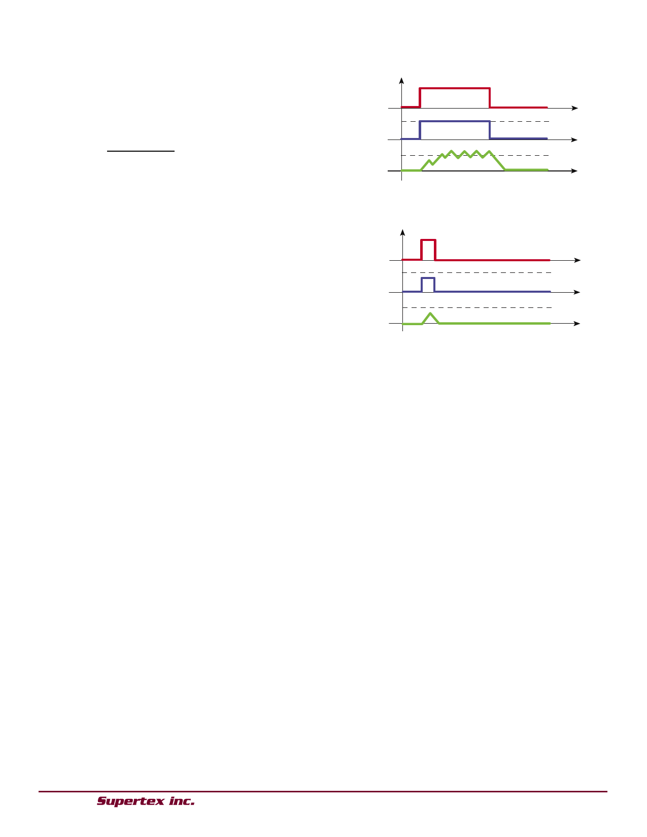
droop in the LED current (Figure. 5; for a CCM design).
Figure 5a: PWM Dimming with dimming on-time far
greater than one switching time period
PWMD
ILED
IINDUCTOR
IO(SS)
IL(SS)
Figure 5b: PWM Dimming with dimming on-time equal
to one switching time
In the above figures, IO(SS) and IL(SS) refer to the steady
state values (PWMD = 100%) for the output current and
inductor current respectively. As can be seen, the inductor
current does not rise enough to trip the CS comparator. This
causes the closed loop amplifier to lose control of the LED
current and COMP rails to VDD.
In the HV9963, however, this problem is overcome by keep-
ing the boost converter ON, even though PWMD has gone
to zero to ensure enough power is delivered to the output.
Thus, the amplifier still has control over the LED current and
the LED current will be in regulation as shown in Figure. 6.
When the PWM signal is high, the GATE and FLT pins are
enabled and the output of the transconductance op-amp
is connected to the external compensation network. Thus,
the internal amplifier controls the output current. When the
PWMD signal goes low, the output of the transconductance
amplifier is disconnected from the compensation network.
Thus, the integrating capacitor maintains the voltage across
it. The FLT pin goes low, turning off the disconnect switch.
However, the boost FET is kept running.
● 1235 Bordeaux Drive, Sunnyvale, CA 94089 ● Tel: 408-222-8888 ● www.supertex.com
9
Share Link: 