LR745 Ver la hoja de datos (PDF) - Microchip Technology
Número de pieza
componentes Descripción
Fabricante
LR745 Datasheet PDF : 15 Pages
| |||
LR745
4.0 DESIGN CONSIDERATIONS
To ensure the best design using LR745, evaluate the
value of C1 and the SMPS requirements.
4.1 Calculating the value for C1
Sizing the VCC capacitor, C1, is an important factor.
Making C1 too large will cause the SMPS to power up
too slowly. However, if too small, C1 will not allow the
SMPS to power up due to insufficient charge in the
capacitor to power the IC and MOSFET until the auxil-
iary supply is available. The value of C1 can be approx-
imated by the following equation:
C1 = -V----S---1-Tf---A---R----T---N-–----V----M-1---I-N--
Definitions:
- f = switching frequency
- N = number of clock cycles required to
charge VAUX to VMIN value
- I = PWM operating current
- VSTART = PWM IC start threshold rating
- VMIN = PWM IC minimum VCC operating volt-
age
Consider for example, a PWM IC with a switching fre-
quency of 100KHz, operating current of 20mA, start
threshold of 16V, and a minimum operating voltage of
10V. If 100 clock cycles are required to charge the aux-
iliary voltage to 10V, the minimum value of C1 is calcu-
lated as follows:
C1 = ---1--------0------0-----1---k------H----1------z6-----V------–-1---1-0--0-0---V------2---0----m------A--
4.2 SMPS with wide minimum to
maximum load
An important point is that the LR745’s output voltage,
VOUT, must discharge to below the nominal VOFF trip
point of 13.25V in order for its output to turn off. If the
SMPS requires a wide minimum to maximum output
load variation, it will be difficult to guarantee that VCC
will fall below 13.25V under minimum load conditions.
Consider an SMPS that is required to power small as
well as large loads and is also required to power up
quickly. Such a SMPS may power up too fast with a
small load, not allowing the VCC voltage to fall below
13.25V. For such conditions, the circuit in Figure 4-1 is
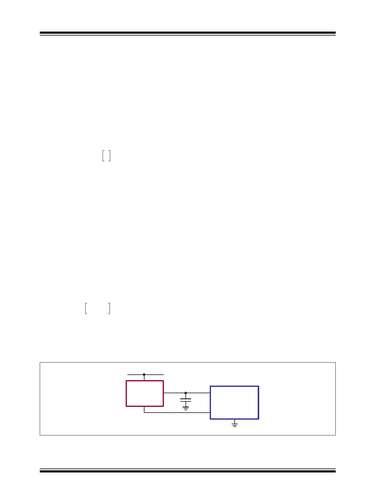
recommended.
In Figure 4-1, the VREF pin of the UC3844 is used to
bias the ground pin of the LR745. The VREF pin on the
UC3844 is a 5.0V reference, which stays at 0V until the
VCC voltage reaches the start threshold voltage. Once
VCC reaches the start threshold voltage, VREF will
switch digitally from 0V to 5.0V. During start-up, the
LR745 will be on, and VCC will start to increase up to
16V. Once VCC reaches16V, the UC3844 will start to
operate and VREF will increase from 0V to 5.0V. The
LR745 will see an effective VOUT voltage of 11V (16V
minus 5.0V) because the ground of the LR745 is now
at 5.0V. The LR745 will immediately turn off its output,
VOUT, without having to wait for the VCC voltage to
decrease. The VREF switching from 0 to 5.0V during
start is a common feature in most PWM ICs.
C1 = 3.3F
FIGURE 4-1:
USING VREF FOR GROUND VOLTAGE
VIN
LR7
GND
VOUT
C1
VCC
VREF
PWM IC
DS20005394A-page 8
2015 Microchip Technology Inc.
Share Link: 