LTC1064-7 Ver la hoja de datos (PDF) - Linear Technology
Número de pieza
componentes Descripción
Fabricante
LTC1064-7 Datasheet PDF : 12 Pages
| |||
LTC1064-7
APPLICATI S I FOR ATIO
Speed Limitations
To avoid op amp slew rate limiting at maximum clock
frequencies, the signal amplitude should be kept below a
specified level as shown in Table 9.
Transient Response
Table 9. Maximum VIN vs VS and Clock
POWER SUPPLY
±7.5V
±5V
Single 5V
MAXIMUM fCLK
5.0MHz
4.5MHz
4.0MHz
≥ 3.5MHz
3.5MHz
≥ 3.0MHz
2.0MHz
MAXIMUM VIN
1.8VRMS (fIN > 80kHz)
2.3VRMS (fIN > 80kHz)
2.7VRMS (fIN > 80kHz)
1.4VRMS (fIN > 500kHz)
1.6VRMS (fIN > 80kHz)
0.7VRMS (fIN > 400kHz)
0.5VRMS (fIN > 250kHz)
Table 10. Transient Response of LTC Lowpass Filters
LOWPASS FILTER
DELAY
TIME*
(SEC)
RISE SETTLING
TIME** TIME***
(SEC) (SEC)
LTC1064-3 Bessel
0.50/fC 0.34/fC 0.80/fC
LTC1164-5 Bessel
0.43/fC 0.34/fC 0.85/fC
LTC1164-6 Bessel
0.43/fC 0.34/fC 1.15/fC
LTC1264-7 Linear Phase 1.15/fC 0.36/fC 2.05/fC
LTC1164-7 Linear Phase 1.20/fC 0.39/fC 2.2/fC
LTC1064-7 Linear Phase 1.20/fC 0.39/fC 2.2/fC
LTC1164-5 Butterworth
0.80/fC 0.48/fC 2.4/fC
LTC1164-6 Elliptic
0.85/fC 0.54/fC 4.3/fC
LTC1064-4 Elliptic
0.90/fC 0.54/fC 4.5/fC
LTC1064-1 Elliptic
0.85/fC 0.54/fC 6.5/fC
* To 50% ±5%, ** 10% to 90% ±5%, *** To 1% ±0.5%
OVER-
SHOOT
(%)
0.5
0
1
5
5
5
11
18
20
20
Table 11. Aliasing (fCLK = 100kHz)
INPUT FREQUENCY
(VIN = 1VRMS,
fIN = fCLK ± fOUT)
(kHz)
OUTPUT LEVEL
(Relative to Input,
0dB = 1VRMS)
(dB)
50:1, fCUTOFF = 2kHz
190 (or 210)
195 (or 205)
196 (or 204)
197 (or 203)
198 (or 202)
199.5 (or 200.5)
–76.1
– 51.9
– 36.3
– 18.4
– 3.0
– 0.2
100:1, fCUTOFF = 1kHz
97 (or 103)
97.5 (or 102.5)
98 (or 102)
98.5 (or 101.5)
99 (or 101)
–74.2
– 53.2
– 36.9
– 19.6
– 5.2
99.5 (or 100.5)
– 0.7
OUTPUT FREQUENCY
(Aliased Frequency
fOUT = ABS [fCLK ± fIN])
(kHz)
10.0
5.0
4.0
3.0
2.0
0.5
3.0
2.5
2.0
1.5
1.0
0.5
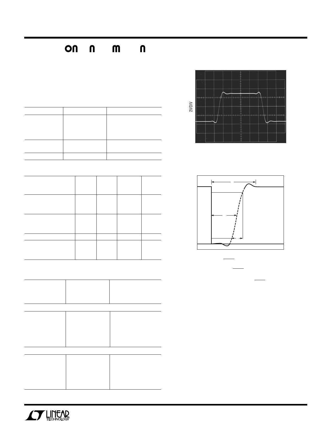
50µs/DIV
VS = ±7.5V, fIN = 2kHz ± 3V
fCLK = 1MHz, RATIO = 50:1
Figure 5.
ts
INPUT
90%
1064-7 F05
OUTPUT
50%
td
10%
tr
RISE
TIME
(tr)
=
0.39
fCUTOFF
±
5%
SETTLING
(TO 1% of
TIME (ts)
OUTPUT)
=
2.2
fCUTOFF
±5%
DELAY TIME (td) = GROUP
(TO 50% OF OUTPUT)
DELAY
≈
1.2
fCUTOFF
1064-7 F06
Figure 6.
Aliasing
Aliasing is an inherent phenomenon of sampled data
systems and it occurs when input frequencies close to the
sampling frequency are applied. For the LTC1064-7 case
at 100:1, an input signal whose frequency is in the range
of fCLK ±3%, will be aliased back into the filter’s passband.
If, for instance, an LTC1064-7 operating with a 100kHz
clock and 1kHz cutoff frequency receives a 98kHz, 10mV
input signal, a 2kHz, 143µVRMS alias signal will appear at
its output. When the LTC1064-7 operates with a clock-to-
cutoff frequency of 50:1, aliasing occurs at twice the clock
frequency. Table 11 shows details.
Information furnished by Linear Technology Corporation is believed to be accurate and reliable.
However, no responsibility is assumed for its use. Linear Technology Corporation makes no represen-
tation that the interconnection of its circuits as described herein will not infringe on existing patent rights.
11
Share Link: 