UPD4713AGT Ver la hoja de datos (PDF) - NEC => Renesas Technology
Número de pieza
componentes Descripción
Fabricante
UPD4713AGT Datasheet PDF : 16 Pages
| |||
µPD4713A
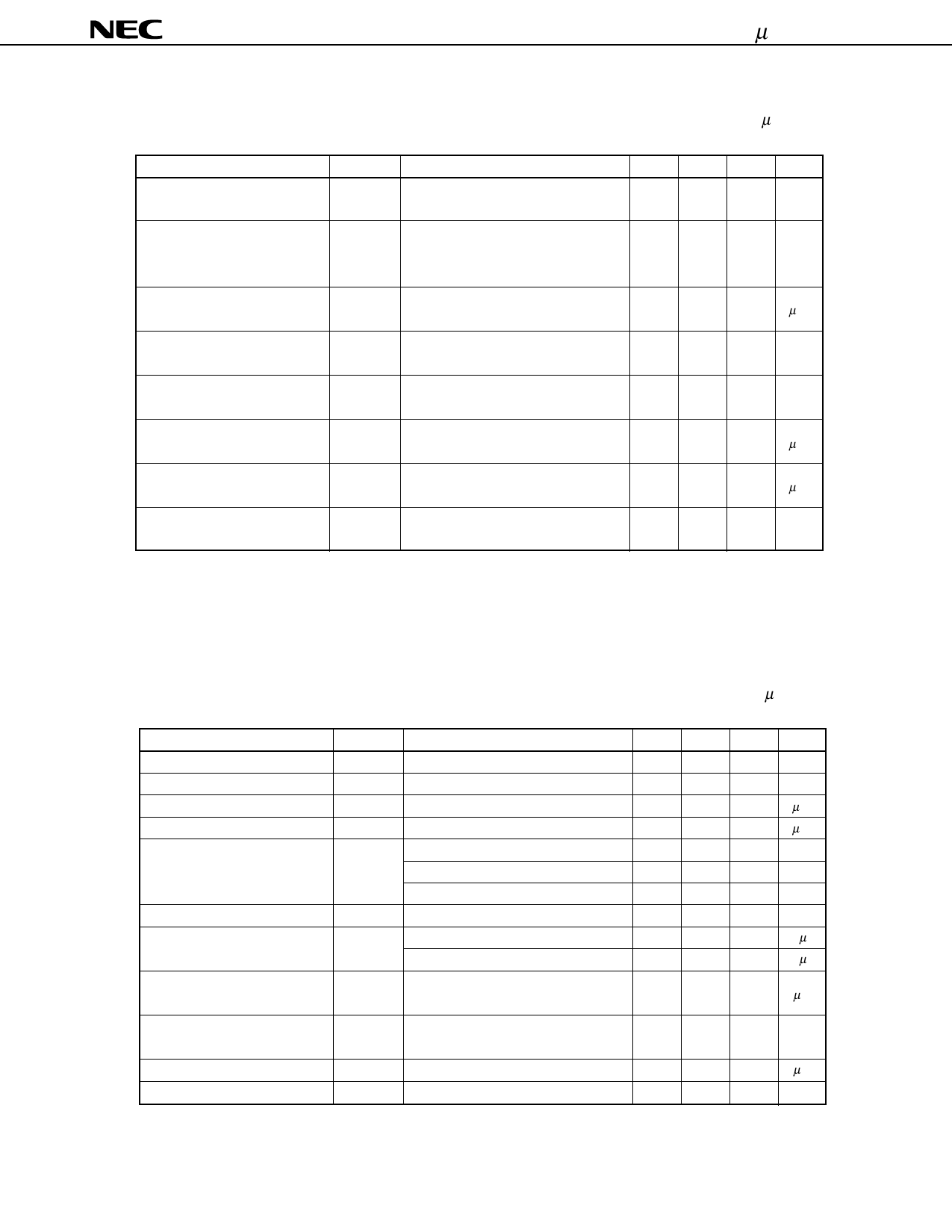
ELECTRICAL CHARACTERISTICS (OVERALL)
(Unless otherwise specified, VCC = +5 V ±10 %, TA = –20 ˚C to +80 ˚C, C1 to C4 = 22 µF)
Parameter
Circuit current
Circuit current
Standby circuit current
Standby low-level
input voltage
Standby high-level
input voltage
Standby high-level
input current
Standby low-level
input current
Input capacitance
Symbol
Conditions
MIN.
VCC = +5 V, no load, RIN pin open
ICC1
(Standby pin open)
VCC = +5 V, RL = 3 kΩ (DOUT), DIN = GND,
ICC2
RIN and ROUT pins open
(Standby pin open)
ICC
VCC = +5 V, no load, RIN pin open
(Standby) (Standby pin high)
VIL
Note 3
(Standby)
VIH
(Standby)
2.0
IIH
VCC = +5.5 V
(Standby) VI = 5.5 V
IIL
VCC = +5.5 V
(Standby) VI = 0 V
Driver input and receiver input
CIN
VCC = +5 V, vs. GND, f = 1 MHz
TYP.
5.0
21.0
50
MAX. Unit
18.0 mA
40.0 mA
120 µA
0.8 V
V
100 µA
–1 µA
10 pF
* TYP.: Typical (reference) value at TA = 25 ˚C.
Note 3. Because the standby pin is internally pulled down, if the standby pin is left open, operating mode is in
effect.
ELECTRICAL CHARACTERISTICS (DRIVER)
(Unless otherwise specified, VCC = +5 V ±10 %, TA = –20 ˚C to +80 ˚C, C1 to C4 = 22 µF)
Parameter
Low-level input voltage
High-level input voltage
Low-level input current
High-level input current
Output voltage
Output short current
Slew rate
Propagation delay time Note 4
Output resistance
Standby output transition time
Standby output transition time
Symbol
VIL
VIH
IIL
IIH
VDO
ISC
SR
tPHL
tPLH
RO
tDAZ
tDZA
Conditions
VCC = +5.0 V, RL = ∞, TA = 25 ˚C
VCC = +5.0 V, RL = 3 kΩ
VCC = +4.5 V, RL = 3 kΩ
VCC = +5.0 V, vs. GND
CL = 10 pF, RL = 3 to 7 kΩ
CL = 2500 pF, RL = 3 to 7 kΩ
RL = 3.5 kΩ, CL = 2500 pF
VCC = VDD = VSS = 0 V
VOUT = ±2 V
Note 5
Note 5
* TYP.: Typical (reference) value at TA = 25 ˚C.
MIN.
2.0
0
0
±5.5
±5.0
1.5
1.5
TYP. MAX.
0.8
±9.7
–1.0
1.0
±15 ±40
9
30
4
30
Unit
V
V
µA
µA
V
V
V
mA
V/µs
V/µs
0.8
µs
300 500
Ω
4
10
µs
25
50 ms
5
Share Link: 