LG1605DXB Ver la hoja de datos (PDF) - Agere -> LSI Corporation
Número de pieza
componentes Descripción
Fabricante
LG1605DXB Datasheet PDF : 12 Pages
| |||
Data Sheet
February 1999
LG1605DXB Limiting Amplifier
Pin Information (continued)
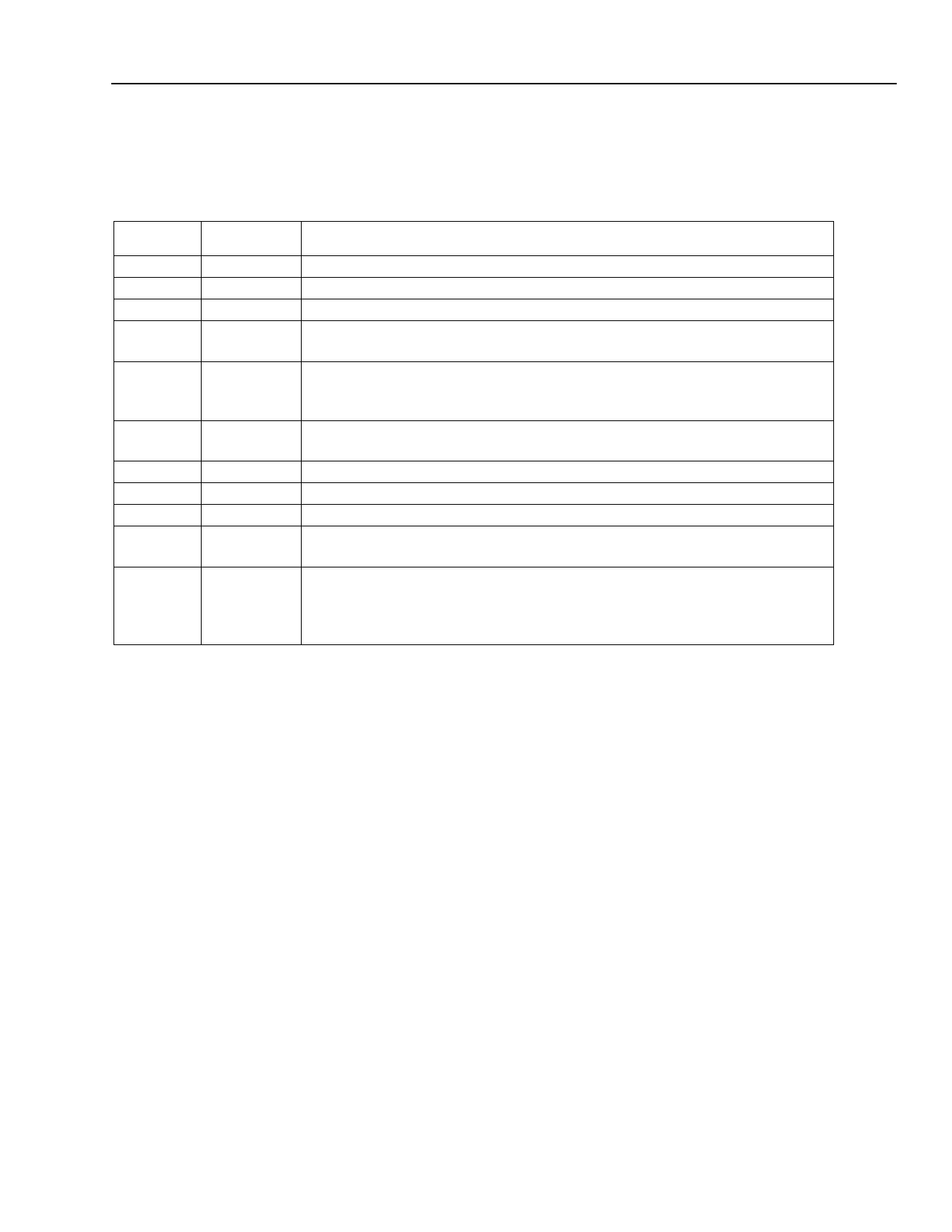
The pin descriptions for the LG1605DXB are given in Table 1.
Table 1. Pin Descriptions
Pin
2
3
7
8
9
10
11
12
13
14
1, 4, 5, 6,
15, 16,
Package
Back
Symbol
V+OUT
V–OUT
VSS
VBR
V–REF
V–IN
V+IN
V+REF
VBF
VBS
GND
Name/Description
Positive Data Output.
Negative Data Output.
dc Supply Voltage.
Bias Reference Voltage. Connect to nominal –1.5 V stable voltage refer-
ence, bypassed to GND with a capacitor ≥0.047 µF.
Data Negative Reference. Internally bypassed with 110 pF. Broadband
operation requires up-close external bypassing with a capacitor ≥0.047 µF,
matching the input coupling capacitor.
Negative Data Input. Requires ac-coupling capacitor and 50 Ω source or
termination.
Positive Data Input.
Data Positive Reference. See pin 9 above.
Bias Force Voltage. Obsolete function, do not connect.
Bias Sense Voltage. Internal test point, tracking VBR. Normally not con-
nected.
Ground. For optimum performance, package back should contact board
ground plane. (See the Mounting and Connections section.)
Lucent Technologies Inc.
3
Share Link: 