PCA9617ADMR2G Ver la hoja de datos (PDF) - ON Semiconductor
Número de pieza
componentes Descripción
Fabricante
PCA9617ADMR2G Datasheet PDF : 15 Pages
| |||
PCA9617A
APPLICATION DESIGN−IN INFORMATION
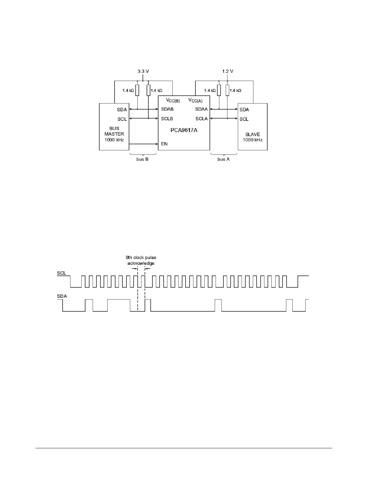
A typical application is shown in Figure 3. In this
example, the system master is running on a 3.3 V I2C−bus
while the slave is connected to a 1.2 V bus. Both buses run
at 1000 kHz. Master devices can be placed on either bus.
Figure 3. Typical Application
The PCA9617A is 5 V tolerant, so it does not require any
additional circuitry to translate between 0.8 V to 5.5 V bus
voltages and 2.2 V to 5.5 V bus voltages.
When port A of the PCA9617A is pulled LOW by a driver
on the I2C−bus, a comparator detects the falling edge when
it goes below 0.3VCC(A) and causes the internal driver on
port B to turn on, causing port B to pull down to about 0.5 V.
When port B of the PCA9617A falls, first a CMOS
hysteresis type input detects the falling edge and causes the
internal driver on port A to turn on and pull the port A pin
down to ground. In order to illustrate what would be seen in
a typical application, refer to Figures 4 and 5. If the bus
master in Figure 3 were to write to the slave through the
PCA9617A, waveforms shown in Figure 4 would be
observed on the A bus. This looks like a normal I2C−bus
transmission except that the HIGH level may be as low as
0.8 V, and the turn on and turn off of the acknowledge signals
are slightly delayed.
Figure 4. Bus A (0.9 V to 5.5 V Bus) Waveform
http://onsemi.com
5
Share Link: 