LT8580 Ver la hoja de datos (PDF) - Linear Technology
Número de pieza
componentes Descripción
Fabricante
LT8580
Linear Technology

LT8580 Datasheet PDF : 32 Pages
| |||
LT8580
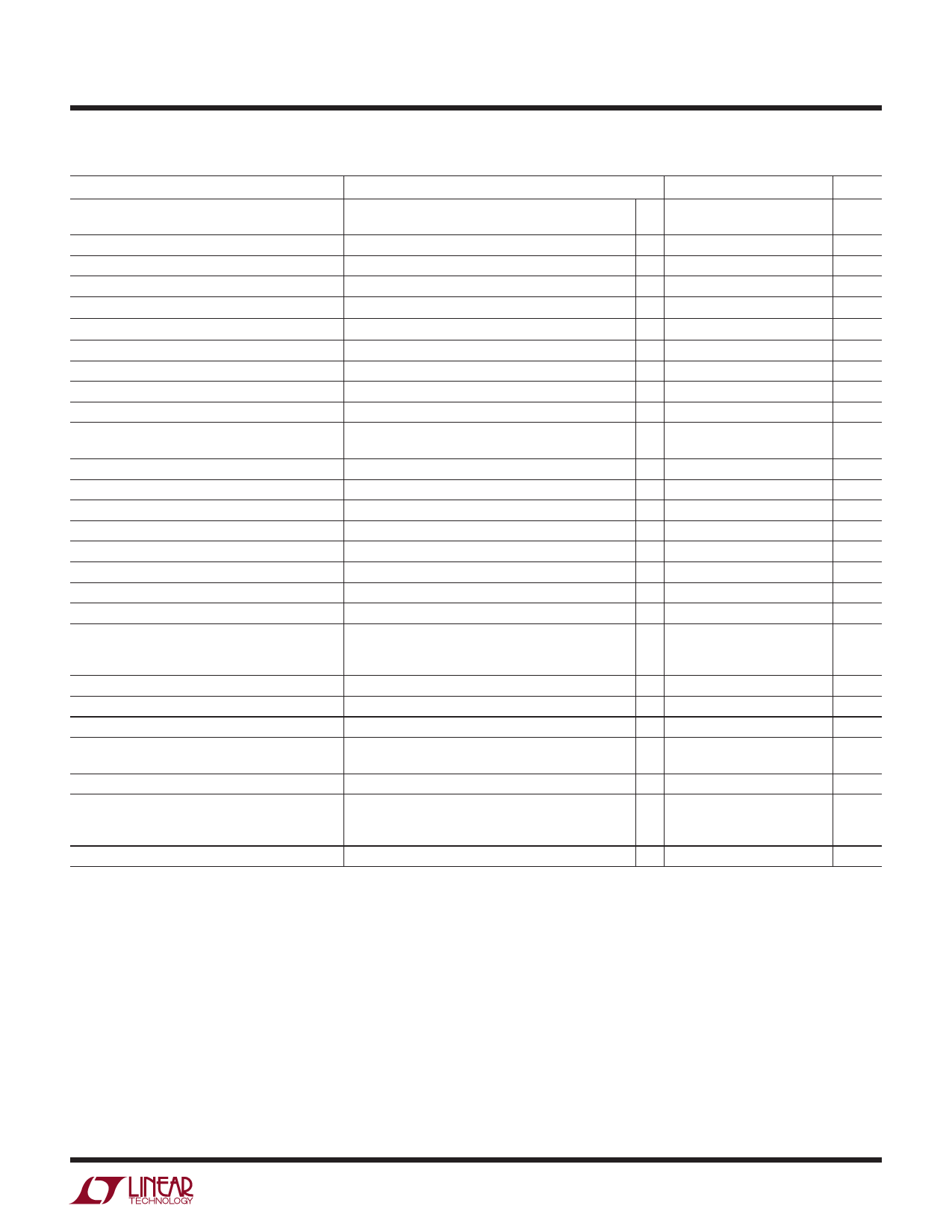
Electrical Characteristics The l denotes the specifications which apply over the full operating
temperature range, otherwise specifications are at TA = 25°C. VIN = 5V, VSHDN = VIN unless otherwise noted. (Note 2)
PARAMETER
CONDITIONS
MIN TYP MAX UNITS
Operating Voltage Range
LT8580E, LT8580I
LT8580H
l 2.55
l 2.9
40
V
40
V
Positive Feedback Voltage
l 1.185 1.204 1.220
V
Negative Feedback Voltage
l –3
3
12
mV
Positive FBX Pin Bias Current
Negative FBX Pin Bias Current
VFBX = Positive Feedback Voltage, Current Into Pin l 81
83.3
85
µA
VFBX = Negative Feedback Voltage, Current Out of Pin l 81
83.3
86
µA
Error Amplifier Transconductance
200
µmhos
Error Amplifier Voltage Gain
60
V/ V
Quiescent Current
Quiescent Current in Shutdown
Reference Line Regulation
Switching Frequency, fOSC
Switching Frequency in Foldback
Switching Frequency Set Range
VSHDN = 2.5V, Not Switching
VSHDN = 0V
2.5V ≤ VIN ≤ 40V
RT = 56.2k
RT = 422k
Compared to Normal fOSC
SYNCing or Free Running
1.2
1.7
mA
0
1
µA
0.01 0.05
%/ V
l 1.23
1.5
1.77
MHz
l 165
200
235
kHz
1/6
Ratio
l 200
1500
kHz
SYNC High Level for Synchronization
l 1.3
V
SYNC Low Level for Synchronization
l
0.4
V
SYNC Clock Pulse Duty Cycle
Recommended Minimum SYNC Ratio fSYNC/fOSC
Minimum Off-Time
VSYNC = 0V to 2V
35
65
%
3/4
100
ns
Minimum On-Time
350
ns
Switch Current Limit
Switch VCESAT
Switch Leakage Current
Soft-Start Charging Current
SHDN Minimum Input
Voltage High
Minimum Duty Cycle (Note 3)
l 1.2
1.5
1.8
A
Maximum Duty Cycle (Notes 3, 4), fOSC = 1.5MHz
l 0.6
1
1.5
A
Maximum Duty Cycle (Notes 3, 4), fOSC = 200kHz
l 0.4
0.8
1.4
A
ISW = 0.75A
400
mV
VSW = 5V
0.01
1
µA
VSS = 0.5V
l
4
6
8
µA
Active Mode, SHDN Rising
l 1.23 1.31
1.4
V
Active Mode, SHDN Falling
l 1.21 1.27 1.33
V
SHDN Input Voltage Low
Shutdown Mode
l
0.3
V
SHDN Pin Bias Current
SHDN Hysteresis
VSHDN = 3V
VSHDN = 1.3V
VSHDN = 0V
44
56
µA
9
12
15
µA
0
0.1
µA
40
mV
Note 1: Stresses beyond those listed under Absolute Maximum Ratings
may cause permanent damage to the device. Exposure to any Absolute
Maximum Rating condition for extended periods may affect device
reliability and lifetime.
Note 2: The LT8580E is guaranteed to meet performance specifications
from 0°C to 125°C junction temperature. Specifications over the –40°C
to 125°C operating junction temperature range are assured by design,
characterization and correlation with statistical process controls. The
LT8580I is guaranteed over the full –40°C to 125°C operating junction
temperature range. The LT8580H is guaranteed over the full –40°C to
150°C operating junction temperature range. Operating lifetime is derated
at junction temperatures greater than 125°C.
Note 3: Current limit guaranteed by design and/or correlation to static test.
Note 4: Current limit measured at equivalent of listed switching frequency.
Note 5: This IC includes overtemperature protection that is intended
to protect the device during momentary overload conditions. Junction
temperature will exceed 150°C when overtemperature protection is active.
Continuous operation above the specified maximum operating junction
temperature may impair device reliability.
8580f
For more information www.linear.com/LT8580
3
Share Link: