FSL4110LR Ver la hoja de datos (PDF) - Fairchild Semiconductor
Número de pieza
componentes Descripción
Fabricante
FSL4110LR Datasheet PDF : 15 Pages
| |||
Functional Description
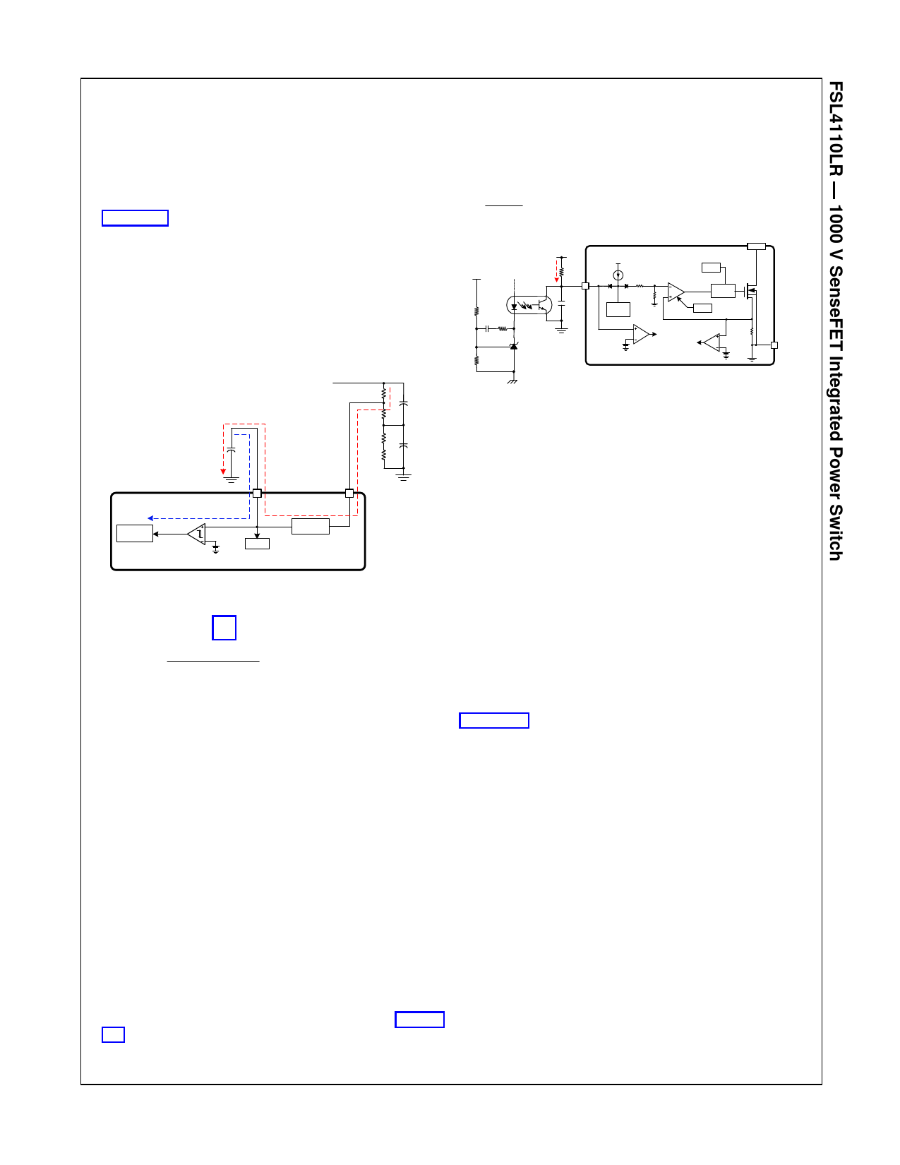
1. Startup and High-Voltage Regulator
During startup, an internal high-voltage current source
(ICH) of the high-voltage regulator (HVREG) supplies the
internal bias current (ISTART) and charges the external
capacitor (CVCC) connected to VCC pin, as shown in
Figure 17. This internal high-voltage current source is
enabled until VCC reaches VSTART (12 V). During steady-
state operation, this internal high-voltage regulator
(HVREG) maintains the VCC with 10 V and provides
operating switching current (IOPS) for all internal circuits.
Therefore, FSL4110LR needs no external bias circuit.
The high-voltage regulator is disabled when VCC
supplied by the external bias is higher than 10 V.
However in the case of self-biasing, power consumption
is increased.
Rectified
Line Input
(VDC)
RSTR
R1
CINH
CVCC
R2
CINL
R3
VCC
2
ISTART or IOPS
Internal
Bias
VCC Good
VSTART VREF
/ VSTOP
VSTR
5
ICH
HVREG
Figure 17. Startup and HVREG Block
The startup resistor (RSTR) can be calculated by the
following equation (1).
RSTR
VDC _ MIN VSTART
ICH
(1)
where, IOPS < ICH < 2 mA,
RSTR + R1 = R2 + R3
2. Feedback Control
FSL4110LR employs current-mode control scheme. An
opto-coupler (such as FOD817) and shunt regulator
(such as KA431) in secondary-side are typically used to
implement the feedback network. Comparing the
feedback voltage with the voltage across RSENSE resistor
makes it possible to control the switching duty cycle.
When the input voltage is increased or the output load
is decreased, reference input voltage of shunt regulator
is increased. If this voltage exceeds internal reference
voltage of shunt regulator, opto-diode’s current of the
opto-coupler increases, pulling down the feedback
voltage and reducing drain current.
2.1. Pulse-by-Pulse Current Limit
Because current-mode control is employed, the peak
current flowing through the SenseFET is limited by the
inverting input of PWM comparator, as shown in Figure
18. Assuming that 100 µA current source (IFB) flows
only through the internal resistors (3R + R = 24 k), the
cathode voltage of diode D2 is about 2.4 V. Since D1 is
© 2014 Fairchild Semiconductor Corporation
FSL4110LR • Rev. 1.3
blocked when feedback voltage (VFB) exceeds 2.4 V,
the maximum voltage of the cathode of D2 is clamped
at this voltage. Therefore, the peak value of the current
of the SenseFET is limited at:
2.4V Sense Ratio
RSENSE
(2)
VOUT
VCC
IDLY
FOD817
RDLY
FB
3
CFB
VREF
IFB
3R
D1 D2
R
Line
Comp.
OSC
PWM
Gate
Driver
LEB
Drain
6,7
KA431
VOLP
OLP
AOCP
RSENSE
VAOCP
1 GND
Figure 18. Pulse Width Modulation Circuit
2.2. Leading Edge Blanking (LEB)
At the instant, the internal SenseFET is turned on, a
high-current spike usually occurs through the
SenseFET, caused by primary-side capacitance and
secondary-side rectifier reverse recovery. Excessive
voltage across the RSENSE resistor leads to incorrect
feedback operation in the current-mode PWM control.
To counter this effect, FSL4110LR employs a leading-
edge blanking (LEB) circuit. This circuit inhibits the
PWM comparator for tLEB (250 ns) after the SenseFET
is turned on.
3. Protection Circuits
The protective functions include Overload Protection
(OLP), Over-Voltage Protection (OVP), Under-Voltage
Lockout (UVLO), Abnormal Over-Current Protection
(AOCP), and Thermal Shutdown (TSD). All of the
protections operate in auto-restart mode as shown in
Figure 19. Since these protection circuits are fully
integrated inside the IC without external components,
reliability is improved without increasing cost and PCB
space. If a fault condition occurs, switching is
terminated and the SenseFET remains off. At the same
time, internal protection timing control is activated to
decrease power consumption and stress on passive
and active components during auto-restart. When
internal protection timing control is activated, VCC is
regulated with 10 V through the internal high-voltage
regulator while switching is terminated. This internal
protection timing control continues until restart time
(1.6 s) duration is finished. After counting to 1.6 s, the
internal high-voltage regulator is disabled and VCC is
decreased. When VCC reaches the UVLO stop voltage,
VSTOP (8 V), the protection is reset and the internal high-
voltage current source charges the VCC capacitor via
the high voltage startup pin (VSTR) again. When VCC
reaches the UVLO start voltage, VSTART (12 V), the
FSL4110LR resumes normal operation. In this manner,
auto-restart function can alternately enable and disable
the switching of the power SenseFET until the fault
condition is eliminated.
www.fairchildsemi.com
9
Share Link: 