FSL4110LR Ver la hoja de datos (PDF) - Fairchild Semiconductor
Número de pieza
componentes Descripción
Fabricante
FSL4110LR Datasheet PDF : 15 Pages
| |||
FB 3
VREF
IFB
3R
D1 D2
R
Line
Comp.
OSC
Drain
6,7
PWM
SQ
RQ
LEB
AOCP
Gate
Driver
AOCP
VAOCP
RSENSE
1 GND
Figure 23. AOCP Circuit
3.3. Over-Voltage Protection (OVP)
If the secondary-side feedback circuit malfunctions or a
solder defect causes an opening in the feedback path,
the current through the opto-coupler transistor becomes
almost zero. Then VFB climbs in a similar manner to the
overload situation, forcing the preset maximum drain
current to flow until the overload protection is triggered.
Because more energy than required is provided to the
output, the output voltage may exceed the rated voltage
before the overload protection is triggered, resulting in
the breakdown of the devices in the secondary side. To
prevent this situation, an OVP circuit is employed. In
general, the VCC is proportional to the output voltage
when the bias-winding is used and the FSL4110LR
uses VCC instead of directly monitoring the output
voltage. If VCC exceeds 24.5 V, an OVP circuit is
triggered, resulting in the termination of the switching
operation. To avoid undesired activation of OVP during
normal operation, VCC should be designed to be below
24.5 V in the normal conditions. The internal OVP
circuit is shown in Figure 24.
FB 3
VREF
IFB
3R
D1 D2
R
Line
Comp.
OSC
PWM
SQ
RQ
LEB
OVP
VCC 2
VOVP
OVP
Drain
6,7
Gate
Driver
RSENSE
1 GND
Figure 24. OVP Circuit
3.4. Thermal Shutdown (TSD)
The SenseFET and control IC integrated on the same
package makes it easier to detect the temperature of
the SenseFET. When the junction temperature exceeds
140°C, thermal shutdown is activated. The FSL4110LR
is restarted when the temperature decreases by 60°C
within tRESTART (1.6 s).
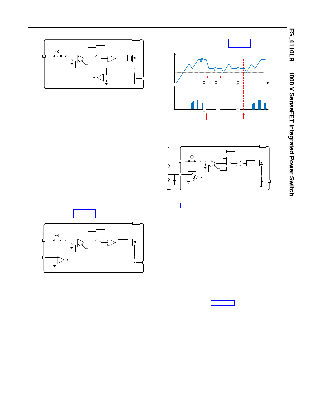
3.5. Line Over-Voltage Protection (LOVP)
If the line input voltage is increased to an undesirable
level, high line input voltage creates high-voltage stress
on the entire system. To protect the SMPS from this
abnormal condition, LOVP is included. It is comprised of
detecting VIN voltage by using divided resistors. When
voltage of VIN voltage is higher than 2.0 V, this condition
is recognized as an abnormal error and PWM switching
shuts down until voltage of VIN voltage decreases to
© 2014 Fairchild Semiconductor Corporation
FSL4110LR • Rev. 1.3
around 1.9 V within tRESTART (see Figure 25). The
internal LOVP circuit is shown in Figure 26.
VCC
VAUX
VSTART
VHVREG
VSTOP
tRESTART
t
IDS
t
LOVP
Occurrence
LOVP
Disappear
Figure 25. LOVP Waveforms
Rectified Line
Input (VDC)
VREF
OSC
IFB
FB 3
3R
PWM
SQ
D1 D2
R
R1
Line
VIN
Comp.
RQ
LEB
LOVP
4
R2
CVIN
VINH
LOVP
Drain
6,7
Gate
Driver
RSENSE
1 GND
Figure 26. LOVP Circuit
Equation (4) calculates the level of input over-voltage to
RMS value.
R2 VINH R1
(4)
VDC VINH
The resistance of divided resistor can be adjusted as
necessary. Small resistance can bring relatively large
stand-by power consumption at light-load condition.
To avoid this situation, a several MΩ resistor is
recommended. For stable operation, a several MΩ
resistor should accompany a capacitor (CVIN) with
hundreds of pF capacitance between the VIN pin and
GND.
4. Oscillator Block
The oscillator frequency is set internally and the
FSL4110LR has a random frequency fluctuation
function as shown in Figure 27. Fluctuation of the
switching frequency can reduce EMI by spreading the
energy over a wider frequency range than the
bandwidth measured by the EMI test equipment. The
range of frequency variation is fixed internally; however,
its selection is randomly chosen by the combination of
an external feedback voltage and an internal free-
running oscillator. This randomly chosen switching
frequency effectively spreads the EMI noise near
switching frequency and allows the use of a cost-
effective inductor instead of an AC input line filter to
satisfy world-wide EMI requirements.
www.fairchildsemi.com
11
Share Link: 