SST25PF040B Ver la hoja de datos (PDF) - Microchip Technology
Número de pieza
componentes Descripción
Fabricante
SST25PF040B Datasheet PDF : 32 Pages
| |||
SST25PF040B
3.0 MEMORY ORGANIZATION
The SST25PF040B SuperFlash memory array is orga-
nized in uniform 4 KByte erasable sectors with 32
KByte overlay blocks and 64 KByte overlay erasable
blocks.
4.0 DEVICE OPERATION
The SST25PF040B is accessed through the SPI (Serial
Peripheral Interface) bus compatible protocol. The SPI
bus consist of four control lines; Chip Enable (CE#) is
used to select the device, and data is accessed through
the Serial Data Input (SI), Serial Data Output (SO), and
Serial Clock (SCK).
The SST25PF040B supports both Mode 0 (0,0) and
Mode 3 (1,1) of SPI bus operations. The difference
between the two modes, as shown in Figure 4-1, is the
state of the SCK signal when the bus master is in
Standby mode and no data is being transferred. The
SCK signal is low for Mode 0 and SCK signal is high for
Mode 3. For both modes, the Serial Data In (SI) is sam-
pled at the rising edge of the SCK clock signal and the
Serial Data Output (SO) is driven after the falling edge
of the SCK clock signal.
CE#
MODE 3
SCK MODE 0
MODE 3
MODE 0
SI
Bit 7 Bit 6 Bit 5 Bit 4 Bit 3 Bit 2 Bit 1 Bit 0
DON'T CARE
MSB
HIGH IMPEDANCE
SO
Bit 7 Bit 6 Bit 5 Bit 4 Bit 3 Bit 2 Bit 1 Bit 0
MSB
25134 SPIprot.0
FIGURE 4-1:
SPI PROTOCOL
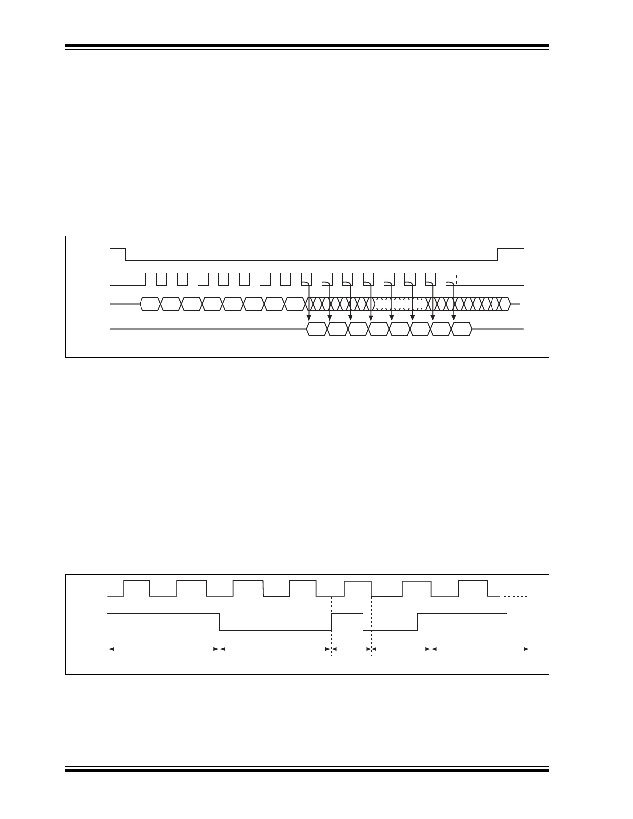
4.1 Hold Operation
The HOLD# pin is used to pause a serial sequence
underway with the SPI flash memory without resetting
the clocking sequence. To activate the HOLD# mode,
CE# must be in active low state. The HOLD# mode
begins when the SCK active low state coincides with
the falling edge of the HOLD# signal. The HOLD mode
ends when the HOLD# signal’s rising edge coincides
with the SCK active low state.
If the falling edge of the HOLD# signal does not coin-
cide with the SCK active low state, then the device
enters Hold mode when the SCK next reaches the
active low state. Similarly, if the rising edge of the
HOLD# signal does not coincide with the SCK active
low state, then the device exits in Hold mode when the
SCK next reaches the active low state. See Figure 4-2
for Hold Condition waveform.
Once the device enters Hold mode, SO will be in high-
impedance state while SI and SCK can be VIL or VIH.
If CE# is driven active high during a Hold condition, it
returns the device to Standby mode. As long as HOLD#
signal is low, the memory remains in the Hold condition.
To resume communication with the device, HOLD#
must be driven active high, and CE# must be driven
active low. See Figure 5-3 for Hold timing.
SCK
HOLD#
Active
Hold
Active
Hold
FIGURE 4-2:
HOLD CONDITION WAVEFORM
Active
25134 HoldCond.0
DS25134A-page 4
2012 Microchip Technology Inc.
Share Link: 