EVAL-AD5755-1SDZ Ver la hoja de datos (PDF) - Analog Devices
Número de pieza
componentes Descripción
Fabricante
EVAL-AD5755-1SDZ Datasheet PDF : 16 Pages
| |||
UG-244
SELECTING THE DEVICE
Figure 6. Device Selection
In the top left corner of the main window, select the main
device on the board, either AD5755, AD5755-1, orAD5757,
from the drop-down list (see Figure 6) to adjust the available
controls accordingly.
ENABLING THE OUTPUT CORRECTLY
To correctly write to and set up the part from a power-on
condition, use the following sequence.
1. Perform a hardware or software reset after initial power-on.
2. The dc-to-dc converter supply block must be configured.
Set the dc-to-dc switching frequency, maximum output
voltage allowed, and the phase that the four dc-to-dc
channels clock at.
3. Configure the DAC control register on a per channel basis.
The output range is selected, and the dc-to-dc converter
block is enabled (DC_DC bit). Other control bits can be
configured at this point. Set the INT_ENABLE bit; however,
the output enable bit (OUTEN) should not be set.
4. Write the required code to the DAC data register. This
implements a full DAC calibration internally. Allow at least
200 µs before Step 5 for reduced output glitch.
5. Write to the DAC control register again to enable the
output (set the OUTEN bit).
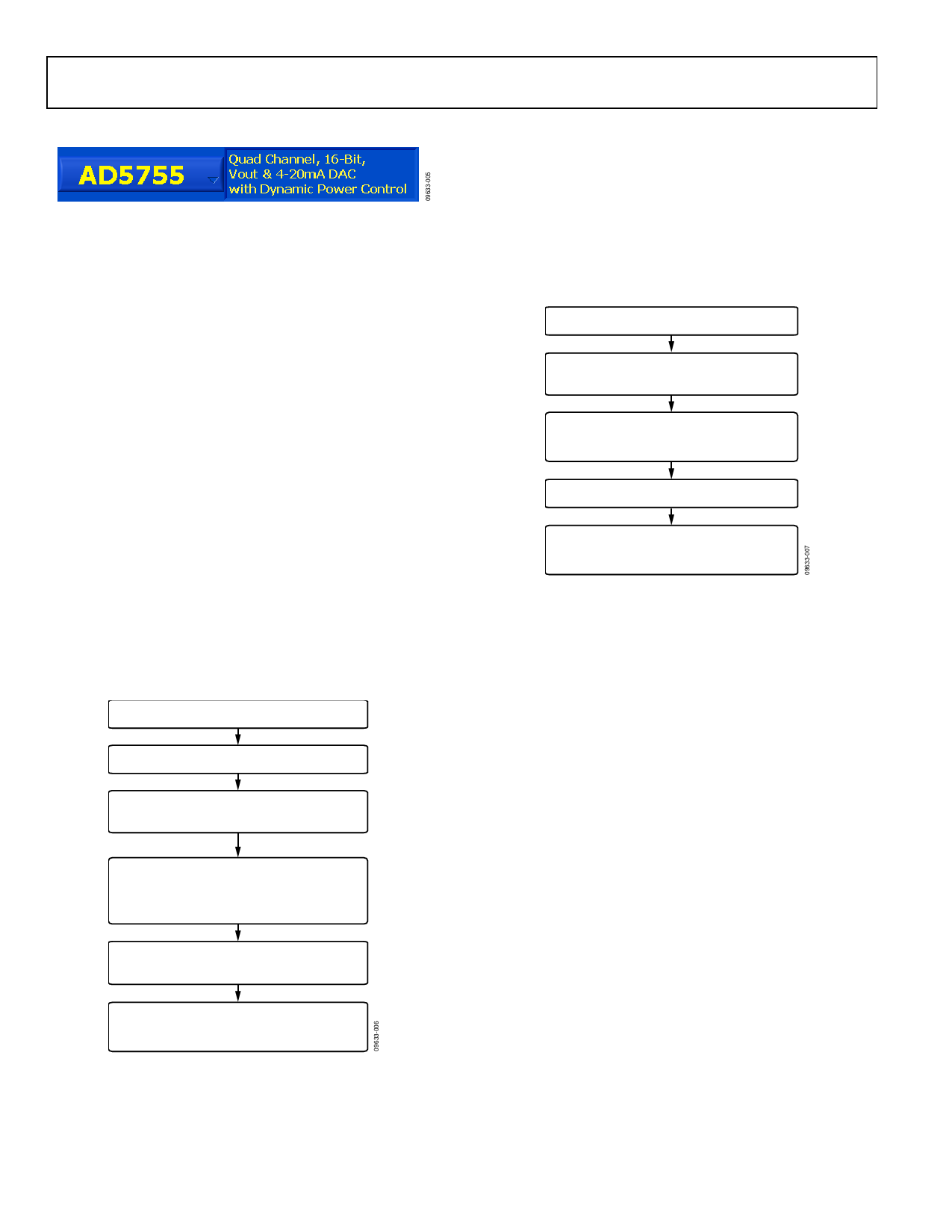
A flowchart of this sequence is shown in Figure 7.
POWER ON.
STEP 1: PERFORM A SOFTWARE/HARDWARE RESET.
STEP 2: WRITE TO DC-TO-DC CONTROL REGISTER TO
SET DC-TO-DC CLOCK FREQUENCY, PHASE,
AND MAXIMUM VOLTAGE.
STEP 3: WRITE TO DAC CONTROL REGISTER. SELECT
THE DAC CHANNEL AND OUTPUT RANGE.
SET THE DC_DC BIT AND OTHER CONTROL
BITS AS REQUIRED. SET THE INT_ENABLE BIT
BUT DO NOT SELECT THE OUTEN BIT.
STEP 4: WRITE TO EACH/ALL DAC DATA REGISTERS.
ALLOW AT LEAST 200µs BETWEEN STEP 3
AND STEP 5 FOR REDUCED OUTPUT GLITCH.
STEP 5: WRITE TO DAC CONTROL REGISTER. RELOAD
SEQUENCE AS IN STEP 3 ABOVE. THIS TIME
SELECT THE OUTEN BIT TO ENABLE
THE OUTPUT.
Figure 7. Programming Sequence for Enabling the Output Correctly
Evaluation Board User Guide
CHANGING AND REPROGRAMMING THE RANGE
When changing between ranges, the same sequence as
described in the Enabling the Output Correctly section should
be used. It is recommended to set the range to its zero point
(can be midscale or zero scale) prior to disabling the output.
Because the dc-to-dc converter switching frequency, maximum
voltage, and phase have already been selected, there is no need
to reprogram these. A flowchart of this sequence is shown in
Figure 8.
CHANNEL’S OUTPUT IS ENABLED.
STEP 1: WRITE TO CHANNEL’S DAC DATA
REGISTER. SET THE OUTPUT
TO 0V (ZERO OR MIDSCALE).
STEP 2: WRITE TO DAC CONTROL REGISTER.
DISABLE THE OUTPUT (OUTEN = 0), AND
SET THE NEW OUTPUT RANGE. KEEP THE
DC_DC BIT AND THE INT_ENABLE BIT SET.
STEP 3: WRITE VALUE TO THE DAC DATA REGISTER.
STEP 4: WRITE TO DAC CONTROL REGISTER.
RELOAD SEQUENCE AS IN STEP 2 ABOVE.
THIS TIME SELECT THE OUTEN BIT TO
ENABLE THE OUTPUT.
Figure 8. Steps for Changing the Output Range
CLEAR COMMAND
To clear an output, each relevant channel must have its clear
code set in the relevant data register (default of 0x0000) and be
enabled for clear operation via the DAC control registers. After
these are set, assert the CLEAR pin to clear the selected channels.
Rev. B | Page 6 of 16
Share Link: 