EVAL-AD5755-1SDZ Ver la hoja de datos (PDF) - Analog Devices
Número de pieza
componentes Descripción
Fabricante
EVAL-AD5755-1SDZ Datasheet PDF : 16 Pages
| |||
Evaluation Board User Guide
UG-244
EVALUATION BOARD HARDWARE
POWER SUPPLIES
The following power supplies are required.
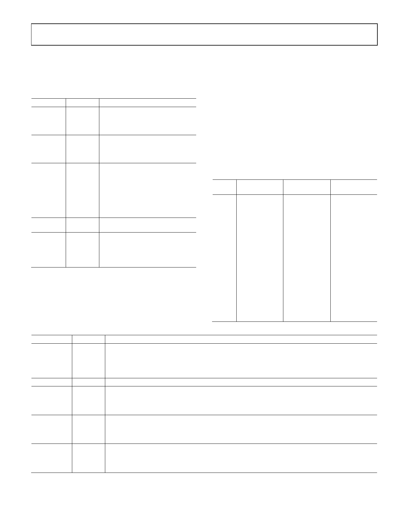
Table 1. Power Supply Connections
Connector Nominal Comment
AVDD
15 V
Positive analog supply voltage.
10.8 V to 33 V range.
(Green LED D2 lights up when power
is supplied to AVDD.)
AVSS
−15 V/
Negative analog supply voltage.
+0 V
+10.8 V to −26.4 V range, or 0 V for
the AD5757 or AD5755-1 in unipolar
supply mode.
AVCC
5V
DC-to-dc supply voltage.
4.5 V to 5.5 V range.
The AVCC input supplies all four on-
board dc-to-dc blocks and may draw
as much as 0.8 A peak current per
channel, depending on the
configuration (see the device data
sheet for more information).
DVDD
3.3 V
Supplied from the SDP connector.
2.7 V to 5.5 V range.
REFIN
5V
See Table 3 for selecting the
reference source: the AD575x
internal reference, the on-board
ADR02 reference, or externally
provided via the REFIN input.
Both analog AGND and PGND inputs are provided on the
board. The PGND input is for the ground of the dc-to-dc
converter circuitry, and a ground connection for the AVCC
supply should be made at this point. The AGND and PGND
planes are connected at one location on the evaluation board.
The AGND and DGND planes are connected at one location
close to the AD5755, AD5755-1, or AD5757 device. Each
supply is decoupled to the relevant ground plane with
10 μF and 0.1 μF capacitors. Each device supply pin is also
decoupled with a 10 μF and 0.1 μF capacitor pair to the relevant
ground plane.
LINK OPTIONS
The link options on the evaluation board should be set for the
required operating setup before using the board. The functions
of the link options are described in Table 3.
Default Link Option Setup
The default link options are listed in Table 2.
Table 2. Default Link Options
Link AD5755
No.
Link Setup
AD5755-1
Link Setup
LK0 Removed
Removed
LK1 Removed
Removed
LK2 Inserted
Inserted
LK3 Inserted
Inserted
LK4 Inserted
Inserted
LK5 Inserted
Removed
LK6 Inserted
Inserted
LK7 Inserted
Removed
LK8 Inserted
Inserted
LK9 Inserted
Removed
LK10 Inserted
Inserted
LK11 Inserted
Removed
LK12 Removed
Removed
LK13 Removed
Removed
LK14 Removed
Removed
LK15 Removed
Removed
AD5757
Link Setup
Removed
Removed
Inserted
Inserted
Removed
Removed
Removed
Removed
Removed
Removed
Removed
Removed
Removed
Removed
Removed
Removed
Table 3. Link Options
Link No.
Device
LK0, LK1, LK2 All Models
LK3
LK4, LK6
LK10, LK8,
All Models
AD5755,
AD5755-1
LK5, LK7 LK9, AD5755
LK11,
LK12, LK13,
LK14, LK15
All Models
Description
These links select the voltage reference source (only one of these should be inserted at any one time).
LK0 selects the internal voltage reference of the AD575x as the voltage reference source.
LK1 selects an external voltage reference source that can be applied at Connector J7.
LK2 selects the on-board ADR02 as the voltage reference source. The ADR02 is supplied by the AVDD supply
and operates under the same input voltage range as the AVDD input of the AD575x, that is 9 V to 33 V.
Powers the on-board ADR02 5 V reference by connecting the AVDD supply to the ADR02 supply pin.
These links connect the +VSENSE input to VOUT for Channel A, Channel B, Channel C, and Channel D, respectively.
When this link is inserted, the +VSENSE input is connected directly to the VOUTx pin.
When this link is removed, the +VSENSE input is left floating and should be connected to the high-side of the
load resistance external to the evaluation board.
These links connect the +VSENSE input to VOUT for Channel A, Channel B, Channel C, and Channel D, respectively.
When this link is inserted, the +VSENSE input is connected directly to the VOUT pin.
When this link is removed, the +VSENSE input is left floating and should be connected to the high-side of the
load resistance external to the evaluation board.
These links allow connection of an external VBOOST supply. (Remove Resistors R43, R44, R17, and R20 to use this
feature.) When inserted, these connect the VBOOST pin of Channel A, Channel B, Channel C, and Channel D,
respectively, to the AVDD supply.
When removed, the VBOOST supplies are controlled by the dc-to-dc converter circuitry.
Rev. B | Page 3 of 16
Share Link: 