AP3988 Ver la hoja de datos (PDF) - Diodes Incorporated.
Número de pieza
componentes Descripción
Fabricante
AP3988 Datasheet PDF : 13 Pages
| |||
Operation Description (Cont.)
A Product Line of
Diodes Incorporated
AP3988/89/90
Constant Primary Peak Current
The primary ip(t) current is sensed by a current sense resistor RCS as shown in Figure 1.
The current rises up linearly at a rate of:
dip (t) Vbulk(t) ……… (1)
dt
LM
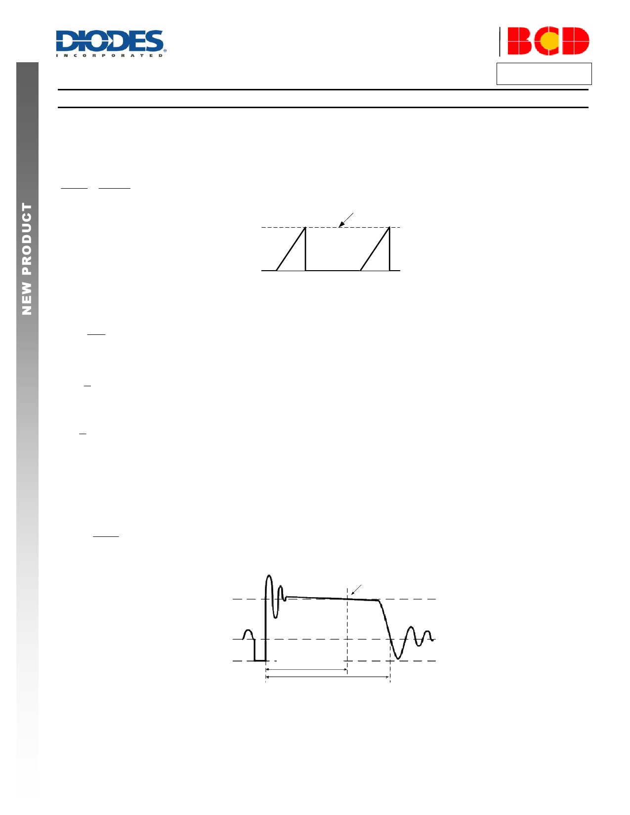
See equation 2
IPK
ip(t)
0A
Figure 2. Primary Current Waveform
As illustrated in Figure 2, when the current ip(t) rises up to IPK, the switch Q1 turns off. The constant peak current is given by:
I PK
VCS
RCS
………(2)
The energy stored in the magnetizing inductance LM each cycle is therefore:
Eg
1
2
LM
I PK 2 ………(3)
So the power transferring from input to output is given by:
P
1
2
LM
IPK2
fSW
………(4)
Where fSW is the switching frequency. When the peak current IPK is constant, the output power depends on the switching frequency fSW.
Constant Voltage Operation
The AP3988/89/90 captures the auxiliary winding feedback voltage at FB pin and operates in constant-voltage (CV) mode to regulate the output
voltage. Assuming the secondary winding is master, the auxiliary winding is slave during the D1 on-time. The auxiliary voltage is given by:
VAUX
N AUX
NS
VO
Vd
………(5)
Where Vd is the diode forward drop voltage, NAUX is the turns of auxiliary winding, and NS is the turns of secondary winding.
See equation 5
VAUX
0V
Portion of Tons
Tons
Figure 3. Auxiliary Voltage Waveform
The output voltage is different from the secondary voltage in a diode forward drop voltage Vd which depends on the current. If the secondary
voltage is always detected at a constant secondary current, the difference between the output voltage and the secondary voltage will be a fixed Vd.
The voltage detection point is portion of Tons after D1 is turned on. The CV loop control function of AP3988/89/90 then generates a D1 off-time to
regulate the output voltage.
AP3988/89/90
Document number: DS36722 Rev. 3 - 2
7 of 13
www.diodes.com
March 2014
© Diodes Incorporated
Share Link: 