ENW89815CXKF Ver la hoja de datos (PDF) - Panasonic Corporation
Número de pieza
componentes Descripción
Fabricante
ENW89815CXKF Datasheet PDF : 34 Pages
| |||
CLASSIFICATION
Einstufung
SUBJECT
Thema
CUSTOMER’S CODE
PAN1455/1555
PRODUCT SPECIFICATION
Produktspezifikation
CLASS 2 BLUETOOTH MODULE
Bluetooth Modul der Klasse 2
PANASONIC’S CODE
ENW89815CxKF/ENW89815AxKF
No.
REV.
DS-1x55-2400-102
1.10
PAGE
Seite
8 of 34
DATE
Datum
27.06.2011
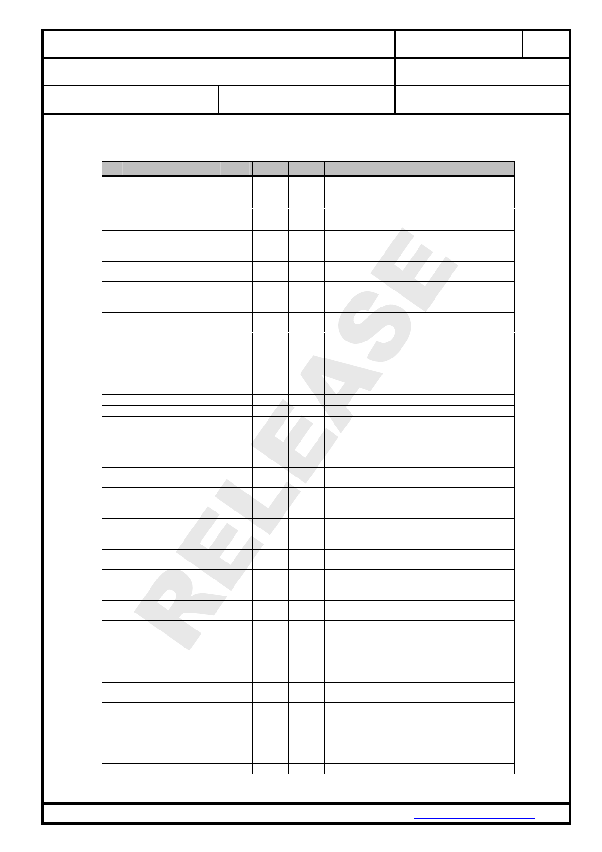
6.1.
GENERAL PIN ASSIGNMENT
No Pin Name
Type PU/PD Active Description
1 GND1
2 ANT
3 UART_RTS#
4 UART_TXD
5 UART_RXD
6 UART_CTS#
7 GPIO[9]/PCM_CLK
P
-
-
I/O -
-
I
PD
H
I
PD
L
O
-
L
O
-
H
I/O PU
L
8 GPIO[10]/PCM_O/TXD3 I/O PU
L
9 GPIO[7]/PCM_SYNC
I/O PD
H
10 GND2
11 ATRST/SPI2_MISO
P
-
-
I/O PU
H
12 GPIO[8]/PCM_I/RXD3 I/O PU
L
13 ATDI/SPI2_CS
I/O PU
-
14 ATMS
15 reserved
16 VCC
17 RESET#
18 GND3
19 GPIO[14]
I
PU
-
I
PD
-
P
-
-
I
PU
L
P
-
-
I/O PU
L
20 GPIO[13]
I/O PD
H
21 GPIO[15]
I/O PU
L
22 GPIO[6]/ADC
I/O PD
H
23 ATDO/SPI2_SCK
24 ATCK
25 GPIO[3]/SPI_CLK
O
PU
-
O
PD
-
I/O PD
H
26 GPIO[0]/SPI_MOSI
I/O PD
H
27 GND4
28 GPIO[2]/SPI_CS
P
-
-
I/O PD
H
29 GPIO[1]/SPI_MISO
I/O PD
H
30 GPIO[5]/TXD2
I/O PD
H
31 GPIO[4]/RXD2
I/O PD
H
32 USB_DM
33 USB_DP
34 GPIO[17]/TAMPER
I/O PD
-
I/O PD
-
I/O PD
-
A GPIO[16]/SPI2_MOSI I/O PU
L
B GPIO[12]/I2C_SCL
I/O PU
L
C GPIO[11]/I2C_SDA
I/O PU
L
D VBAT
P
-
-
Connect to Ground
Antenna Connector
UART Request To Send (active low)
UART Data Input, weak internal Pull-Down
UART Data Output
UART Clear To Send, internal Pull-Up
General Purpose Input/Output, weak internal Pull-
Up / PCM Data Clock Output
General Purpose Input/Output, weak internal Pull-
Up / PCM Data Output/ UART3 DATA Output
General Purpose Input/Output, weak internal Pull-
Down / PCM Data Sync Output
Connect to Ground
JTAG reset, internal Pull-Up / SPI2 Master In -
Slave Out
General Purpose Input/Output, weak internal Pull-
Up / PCM Data Input / UART3 DATA Input
JTAG test data input, weak internal Pull-Up / SPI2
Chip Select
JTAG mode select, weak internal Pull-Up
for Debug-Use only, nc
VCC
Reset input
Connect to Ground
General Purpose Input/Output, weak internal Pull-
Up
General Purpose Input/Output, weak internal Pull-
Down
General Purpose Input/Output, weak internal Pull-
Up
General Purpose Input/Output, weak internal Pull-
Up / ADC Input
JTAG test data output
JTAG clock, weak internal Pull-Down
General Purpose Input/Output, weak internal Pull-
Down / SPI Clock
General Purpose Input/Output, weak internal Pull-
Down / SPI Master Out – Slave In
Connect to Ground
General Purpose Input/Output, weak internal Pull-
Down / SPI Chip Select
General Purpose Input/Output, weak internal Pull-
Down / SPI Master In – Slave Out
General Purpose Input/Output, weak internal Pull-
Down / UART2 DATA Output
General Purpose Input/Output, weak internal Pull-
Down / UART2 DATA Input
USB Data Minus Terminal
USB Data Plus Terminal
General Purpose Input/Output, weak internal Pull-
Down, do not use as current source! / TAMPER In
General Purpose Input/Output, weak internal Pull-
Up / SPI2 Master Out – Slave In
General Purpose Input/Output, weak internal Pull-
Up / I2C Serial Clock Line
General Purpose Input/Output, weak internal Pull-
Up / I2C Serial Data Line
Optional Batterie Backup
Type: PU - Pulled up; PD – pulled down; P – Power; I – Input; O – Output; I/O - bidirectional
PANASONIC ELECTRONIC DEVICES EUROPE GMBH
www.pedeu.pansonic.de
Share Link: 