AT17LV256-10SI(1997) Ver la hoja de datos (PDF) - Atmel Corporation
Número de pieza
componentes Descripción
Fabricante
AT17LV256-10SI Datasheet PDF : 10 Pages
| |||
AT17 Series
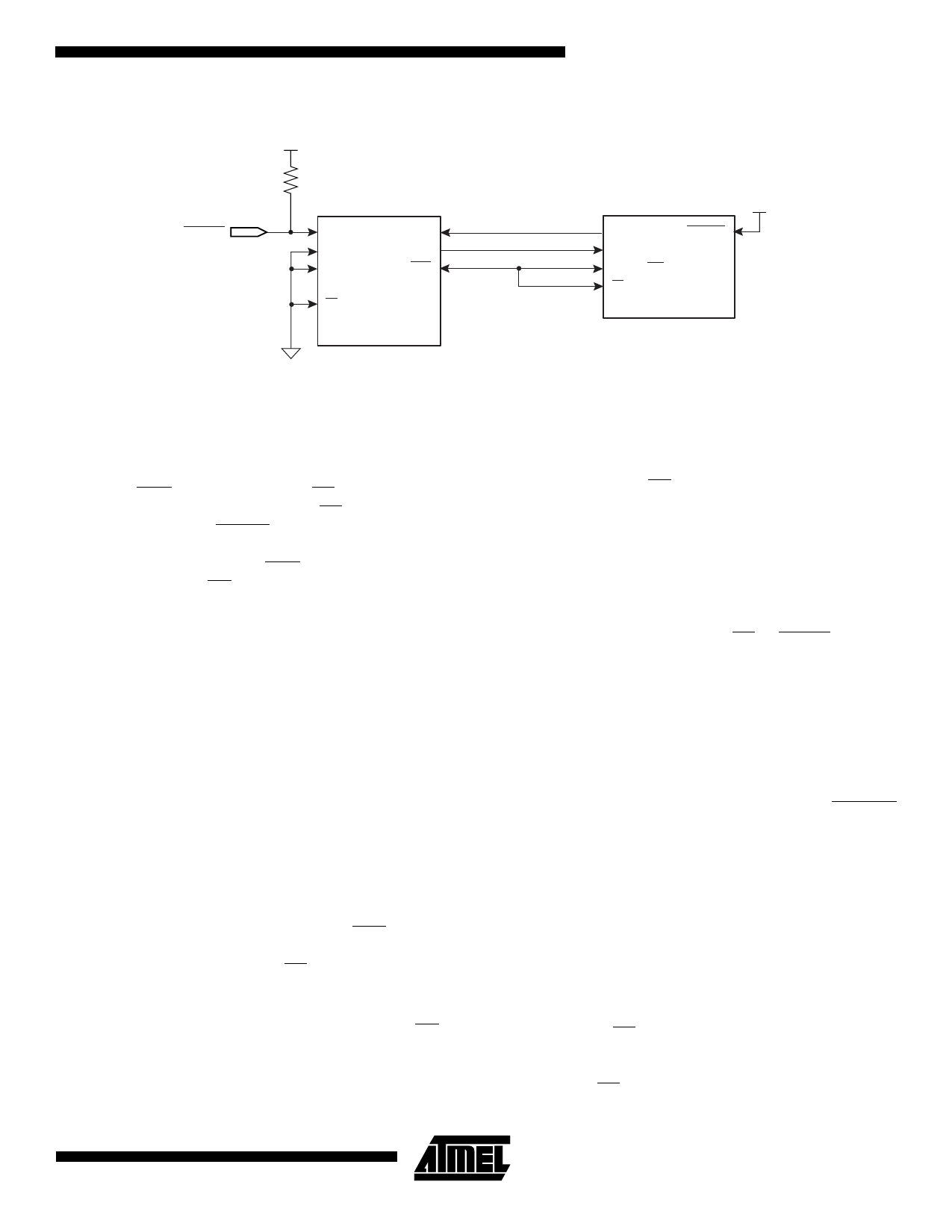
Pin Configurations
PLCC/
SOIC DIP
Pin
Pin Name
I/O Description
2
1
DATA
I/O Three-state DATA output for reading. Input/Output pin for programming.
4
2
CLK
I
Clock input. Used to increment the internal address and bit counter for reading
and programming.
RESET/Output Enable input (when SER_EN is High). A Low level on both the
CE and RESET/OE inputs enables the data output driver. A High level on
6
3
RESET/OE
RESET/OE resets both the addresss and bit counters. A logic polarity of this
input is programmable as either RESET/OE or RESET/OE. This document
describes the pin as RESET/OE.
8
4
CE
I Chip Enable input. Used for device selection. A Low level on both CE and OE
enables the data output driver. A High level on CE disables both the address
and bit counters and forces te device into a low power mode. Note this pin will
not enable/disable the device in 2-wire Serial mode (ie; when SER_EN is Low).
10
5
GND
Ground Pin
14
6
CEO
O Chip Enable Out output. This signal is asserted Low on the clock cycle following
the last bit read from the memory. It will stay Low as long as CE and OE are
both Low. It will then follow CE until OE goes High. Thereafter CEO will stay
High until the entire PROM is read again and senses the status of RESET
polarity.
A2
I Device selection input, A2. This is used to enable (or select) the device during
programming and when SER_EN is Low (see Programming Guide for more
details).
17
7
SER_EN
I
Serial enable is normally high during FPGA loading operations. Bringing
SER_EN low, enables the 2-wire serial interface for programming.
20
8
VCC
+3.3V/+5V power supply pin.
Absolute Maximum Ratings*
Operating Temperature.........................-55°C to +125 °C
Storage Temperature............................-65 °C to +150°C
Voltage on Any Pin
with Respect to Ground.................... -0.1V to VCC + 0.5V
Supply Voltage (Vcc) .............................. -0.5 V to +7.0V
Maximum Soldering Temp. (10 sec. @ 1/16 in.)... 260°C
ESD (RZAP = 1.5K, CZAP = 100pF) ........................2000V
*NOTICE:
Stresses beyond those listed under “Absolute
Maximum Ratings” may cause permanent dam-
age to the device. This is a stress rating only and
functional operation of the device at these or any
other conditions beyond those indicated in the
operational sections of this specification is not
implied. Exposure to absolute maximum rating
conditions for extended periods may affect device
reliability.
3
Share Link: 