74ABT16823A Ver la hoja de datos (PDF) - NXP Semiconductors.
Número de pieza
componentes Descripción
Fabricante
74ABT16823A Datasheet PDF : 12 Pages
| |||
Philips Semiconductors
18-bit bus-interface D-type flip-flop
with reset and enable (3-State)
Product data
74ABT16823A
FEATURES
• Two sets of high speed parallel registers with positive
edge-triggered D-type flip-flops
• Ideal where high speed, light loading, or increased fan-in are
required with MOS microprocessors
• Live insertion/extraction permitted
• Power-up 3-State
• Power-up Reset
• Output capability: +64 mA/–32 mA
• Latch-up protection exceeds 500 mA per Jedec Std 17
• ESD protection exceeds 2000 V per MIL STD 883 Method 3015
and 200 V per Machine Model
DESCRIPTION
The 74ABT16823A 18-bit bus interface register is designed to
eliminate the extra packages required to buffer existing registers and
provide extra data width for wider data/address paths of buses
carrying parity.
The 74ABT16823A has two 9-bit wide buffered registers with Clock
Enable (nCE) and Master Reset (nMR) which are ideal for parity bus
interfacing in high microprogrammed systems.
The registers are fully edge-triggered. The state of each D input, one
set-up time before the LOW-to-HIGH clock transition is transferred
to the corresponding flip-flop’s Q output.
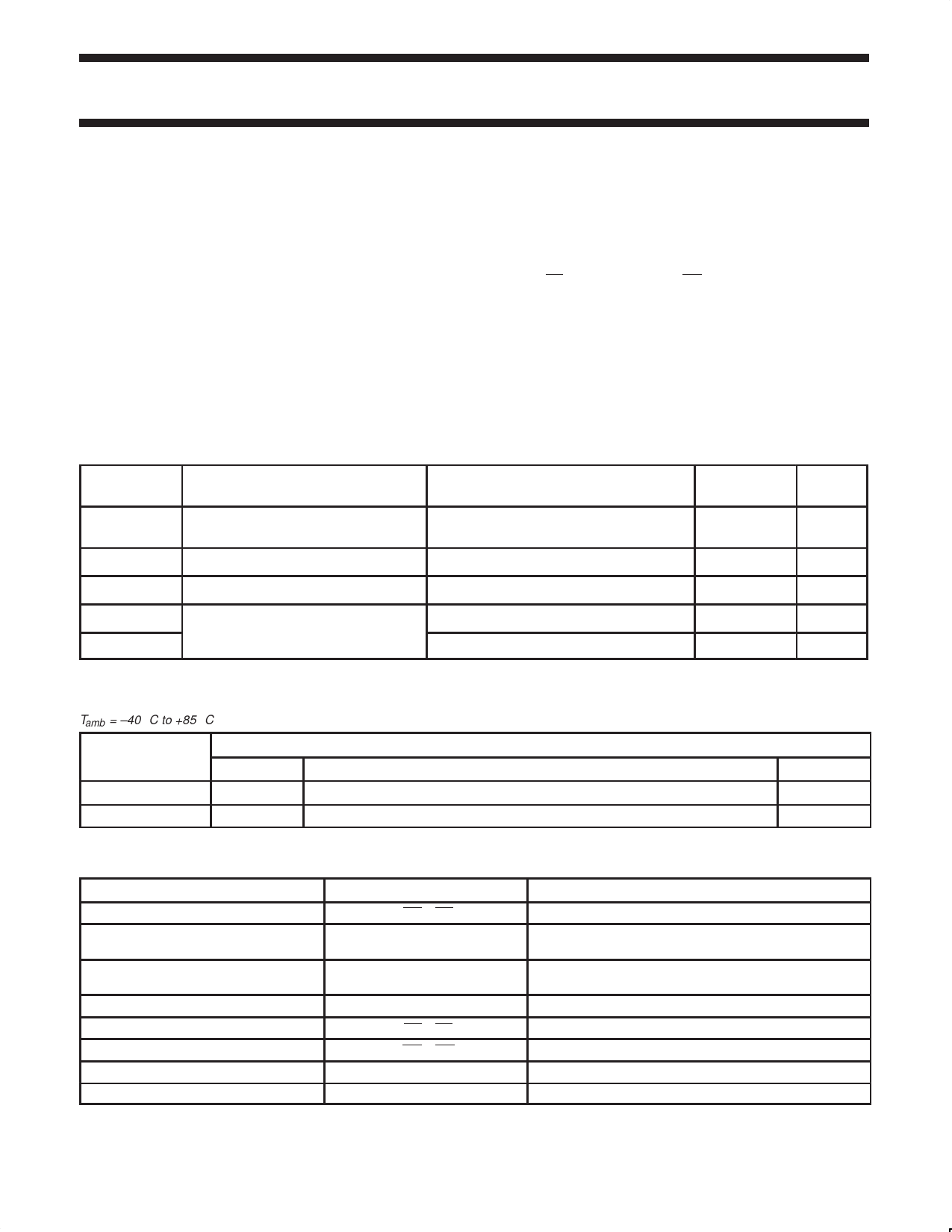
QUICK REFERENCE DATA
SYMBOL
PARAMETER
tPLH
tPHL
CIN
COUT
ICCZ
ICCL
Propagation delay
nCP to nQx
Input capacitance
Output capacitance
Quiescent supply current
CONDITIONS
Tamb = 25 °C; GND = 0 V
CL = 50 pF; VCC = 5 V
VI = 0 V or VCC
VO = 0 V or VCC; 3-State
Outputs disabled; VCC = 5.5 V
Outputs low; VCC = 5.5 V
TYPICAL
2.3
1.9
4
6
500
9
UNIT
ns
pF
pF
µA
mA
ORDERING INFORMATION
Tamb = –40 °C to +85 °C
Type number
Package
Name
74ABT16823ADL
SSOP56
74ABT16823ADGG TSSOP56
Description
plastic shrink small outline package; 56 leads; body width 7.5 mm
plastic thin shrink small outline package; 56 leads; body width 6.1 mm
Version
SOT371-1
SOT364-1
PIN DESCRIPTION
PIN NUMBER
2, 27
54, 52, 51, 49, 48, 47, 45, 44, 43
42, 41, 40, 38, 37, 36, 34, 33, 31
3, 5, 6, 8, 9, 10, 12, 13, 14
15, 16, 17, 19, 20, 21, 23, 24, 26
56, 29
55, 30
1, 28
4, 11, 18, 25, 32, 39, 46, 53
7, 22, 35, 50
SYMBOL
1OE, 2OE
1D0-1D8
2D0-2D8
1Q0-1Q8
2Q0-2Q8
1CP, 2CP
1CE, 2CE
1MR, 2MR
GND
VCC
FUNCTION
Output enable input (active-LOW)
Data inputs
Data outputs
Clock pulse input (active rising edge)
Clock enable input (active-LOW)
Master reset input (active-LOW)
Ground (0 V)
Positive supply voltage
2004 Feb 02
2
Share Link: 