MPF4392 Ver la hoja de datos (PDF) - Motorola => Freescale
Número de pieza
componentes Descripción
Fabricante
MPF4392 Datasheet PDF : 6 Pages
| |||
MPF4392 MPF4393
RGEN
50 Ω
VGEN
SET VDS(off) = 10 V
INPUT
RK
RGG
50 Ω
VGG
–VDD
RD
RT
50 Ω
INPUT PULSE
tr ≤ 0.25 ns
tf ≤ 0.5 ns
PULSE WIDTH = 2.0 µs
DUTY CYCLE ≤ 2.0%
& RGG RK
RD′ = RD(RT + 50)
RD + RT + 50
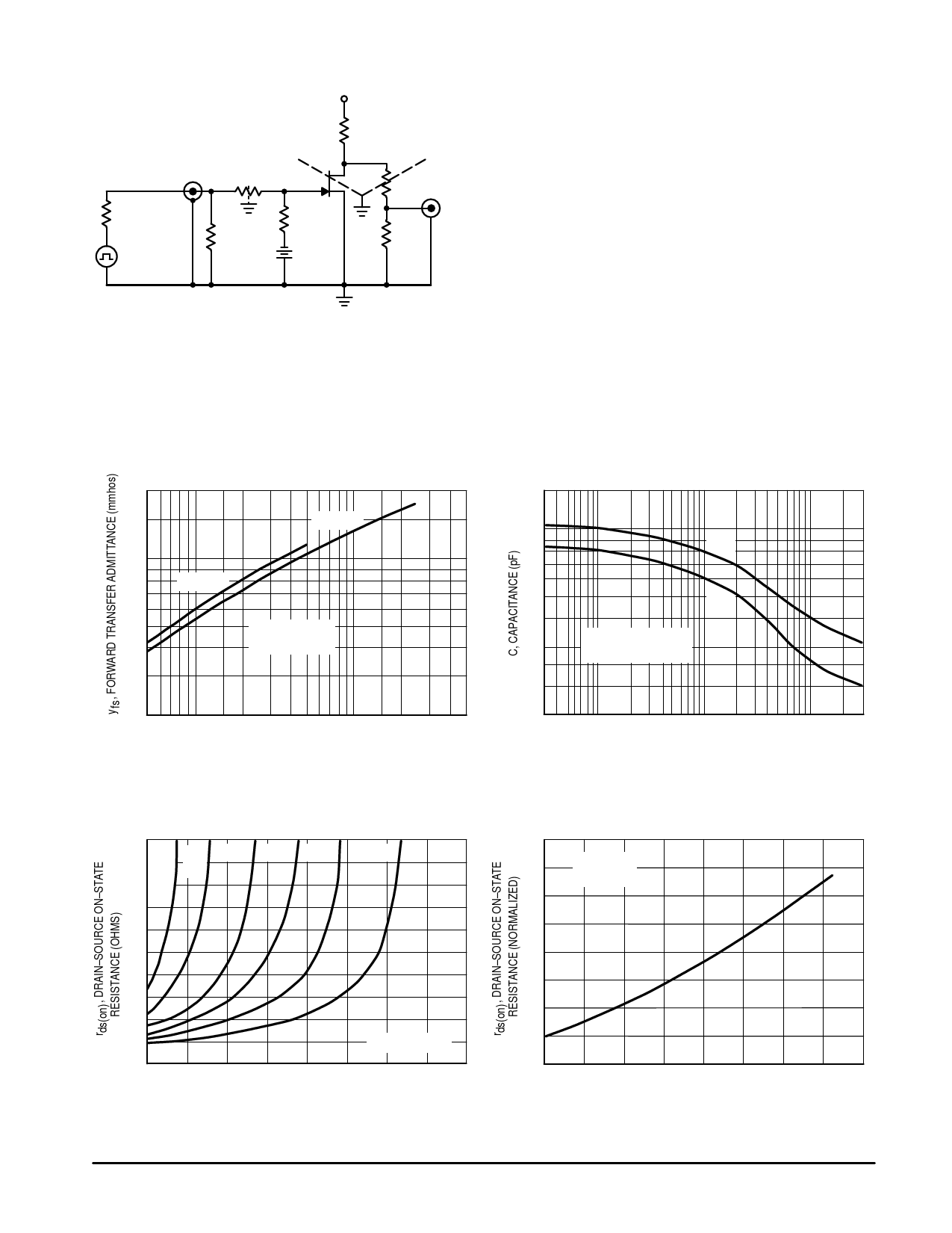
Figure 5. Switching Time Test Circuit
OUTPUT
NOTE 1
The switching characteristics shown above were measured using a
test circuit similar to Figure 5. At the beginning of the switching
interval, the gate voltage is at Gate Supply Voltage (–VGG). The
Drain–Source Voltage (VDS) is slightly lower than Drain Supply
Voltage (VDD) due to the voltage divider. Thus Reverse Transfer
Capacitance (Crss) or Gate–Drain Capacitance (Cgd) is charged to
VGG + VDS.
During the turn–on interval, Gate–Source Capacitance (Cgs)
discharges through the series combination of RGen and RK. Cgd must
discharge to VDS(on) through RG and RK in series with the parallel
combination of effective load impedance (R′D) and Drain–Source
Resistance (rds). During the turn–off, this charge flow is reversed.
Predicting turn–on time is somewhat difficult as the channel
resistance rds is a function of the gate–source voltage. While Cgs
discharges, VGS approaches zero and rds decreases. Since Cgd
discharges through rds, turn–on time is non–linear. During turn–off,
the situation is reversed with rds increasing as Cgd charges.
The above switching curves show two impedance conditions:
1) RK is equal to RD′ which simulates the switching behavior of
cascaded stages where the driving source impedance is normally the
load impedance of the previous stage, and 2) RK = 0 (low impedance)
the driving source impedance is that of the generator.
20
MPF4392
10
MPF4393
7.0
5.0
Tchannel = 25°C
VDS = 15 V
3.0
2.0
0.5 0.7 1.0
2.0 3.0 5.0 7.0 10
20 30 50
ID, DRAIN CURRENT (mA)
Figure 6. Typical Forward Transfer Admittance
15
10
Cgs
7.0
5.0
Cgd
3.0
Tchannel = 25°C
(Cds IS NEGLIGIBLE)
2.0
1.5
1.0
0.03 0.05 0.1
0.3 0.5 1.0
3.0 5.0 10
30
VR, REVERSE VOLTAGE (VOLTS)
Figure 7. Typical Capacitance
200
IDSS 25 50 mA 75 mA 100 mA
= 10 mA
160 mA
125 mA
120
80
40
Tchannel = 25°C
0
0 1.0 2.0 3.0 4.0 5.0 6.0 7.0 8.0
VGS, GATE–SOURCE VOLTAGE (VOLTS)
Figure 8. Effect of Gate–Source Voltage
On Drain–Source Resistance
2.0
1.8
ID = 1.0 mA
VGS = 0
1.6
1.4
1.2
1.0
0.8
0.6
0.4
–70 –40 –10 20 50 80 110 140 170
Tchannel, CHANNEL TEMPERATURE (°C)
Figure 9. Effect of Temperature On
Drain–Source On–State Resistance
Motorola Small–Signal Transistors, FETs and Diodes Device Data
3
Share Link: 