STR-A6359 Ver la hoja de datos (PDF) - Sanken Electric co.,ltd.
Número de pieza
componentes Descripción
Fabricante
STR-A6359 Datasheet PDF : 17 Pages
| |||
STR-A6300 Application Notes
(Ver.1.2)
consumption shall be increased.
When the Vin terminal voltage drops lower than 10.1V(TYP.), the control operation stops by a Under Voltage
Lock Out(UVLO) function and returns to the start-up mode.
Vin
After the control circuit starts its operation, a power
Contro制l c御irc回ui路t o動p作er開ati始on点start point
supply is earned by rectifying and smoothing the voltage
of drive winding D.
17.6V
(typ)
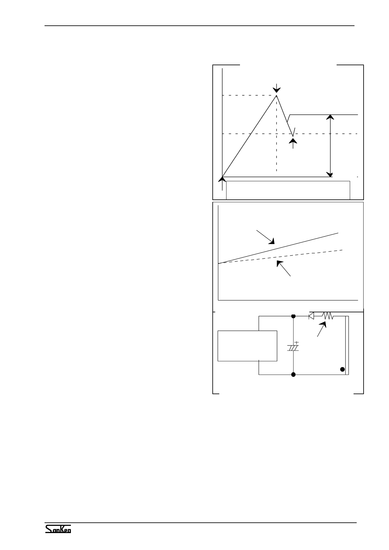
Fig.3 shows the start-up voltage waveform at the
Drive winding voltage
補助巻線電圧
Vin terminal. The drive winding voltage does not
rise up to a set voltage immediately after the control
11.1V
(Max)
circuit starts falling, thanks to the operation stop
voltage set as low as 11.1V(MAX), the drive winding
起Ab動no不rm良al時start up
voltage reaching stabilized voltage before falling to
the operation stop voltage, the control circuit continuing
its operation.
Vin(AC)→ON
図F3ig.起3 W動a時veVfionr端m子of電Vi圧n a波t 形start-up
Time
時間→
The number of windings is to be set at a normal
Vin
power supply operation so that both of the end volts
WRi8tがho無uいt 場R合8
of C2 may be higher than the operation stop voltage
[Vin(OFF) 11.1V(MAX)] and lower than the OVP operating
voltage[Vin(OVP) 23.2V(MIN)].
The preferable drive winding D voltage for stabilization
is 18V approx.. However, in an actual power supply circuit,
there is a case that the Vin terminal voltage varies due to
R8がある場合
With R8
Fig. 4
Iout
the secondary output current as shown on Fig.4.
図4 出力電流Iout ~Vin端子電圧
This is because the circuit current of STR-A6300 series
is small, the C2 being charged up to the peak value by
Vin
the surge voltage generated instantly after the MOSFET
STR-A6300
is turned OFF. In order to prevent this, it is effective to add
R8
a resistor having several to several tens of ohms(R8) in
Gnd
series with the rectifier diode as shown on Fig.5.
The optimum resistance value of the R8 should be
図5 出力電流Ioutの影響を受け難い補助電源回路
Fig.5 Back-up Power Supply Circuit against
determined in accordance with the specs of a
Output current(Io)
transformer since the Vin terminal voltage varies by the structural differences of the transformer.
Furthermore, the variation ratio of the Vin terminal voltage becomes worse due to an inaccurate coupling
between the primary and the secondary winding of the transformer(the coupling between the drive winding D
and the stabilized output winding for the constant voltage control circuitry). Thus, in designing the transformer,
the winding position of the drive winding D should also be studied carefully.
7.2 OCP/FB Terminal (Pin 4), Oscillator and Constant Voltage Control Circuit
The oscillator, making use of charging and discharging of the capacitor incorporated in the IC, generates
pulse signals to determine OFF-time of the MOSFET. The control operation is made by the PRC (Pulse Ratio
Control) operation fixing OFF-time (≒15usec) and varying ON-time of the MOSFET.
Page 9
Share Link: 