STR-A6331 Ver la hoja de datos (PDF) - Sanken Electric co.,ltd.
Número de pieza
componentes Descripción
Fabricante
STR-A6331 Datasheet PDF : 17 Pages
| |||
STR-A6300 Application Notes
(Ver.1.2)
6.3 ELECTRICAL CHARACTERISTICS OF MOSFET(STR-A6351)
Parameter
Ratings
Pin Symbol
Unit
MIN TYP MAX
Drain to source
breakdown voltage
8-1 VDSS
650* -
-
V
Drain leakage current
8-1 IDSS
-
-
300 uA
ON-Resistance
8-1 rDS(ON) -
-
3.95* Ohm
Switching time
8-1 tf
-
-
250 nsec
Thermal resistance
-
Θch- F
-
-
52*
oC /W
*Please refer to each data sheet for details.
Conditions
See each data
sheet.
Channel to
internal frame
7 FUNCTIONS OF EACH TERMINAL AND OPERATION
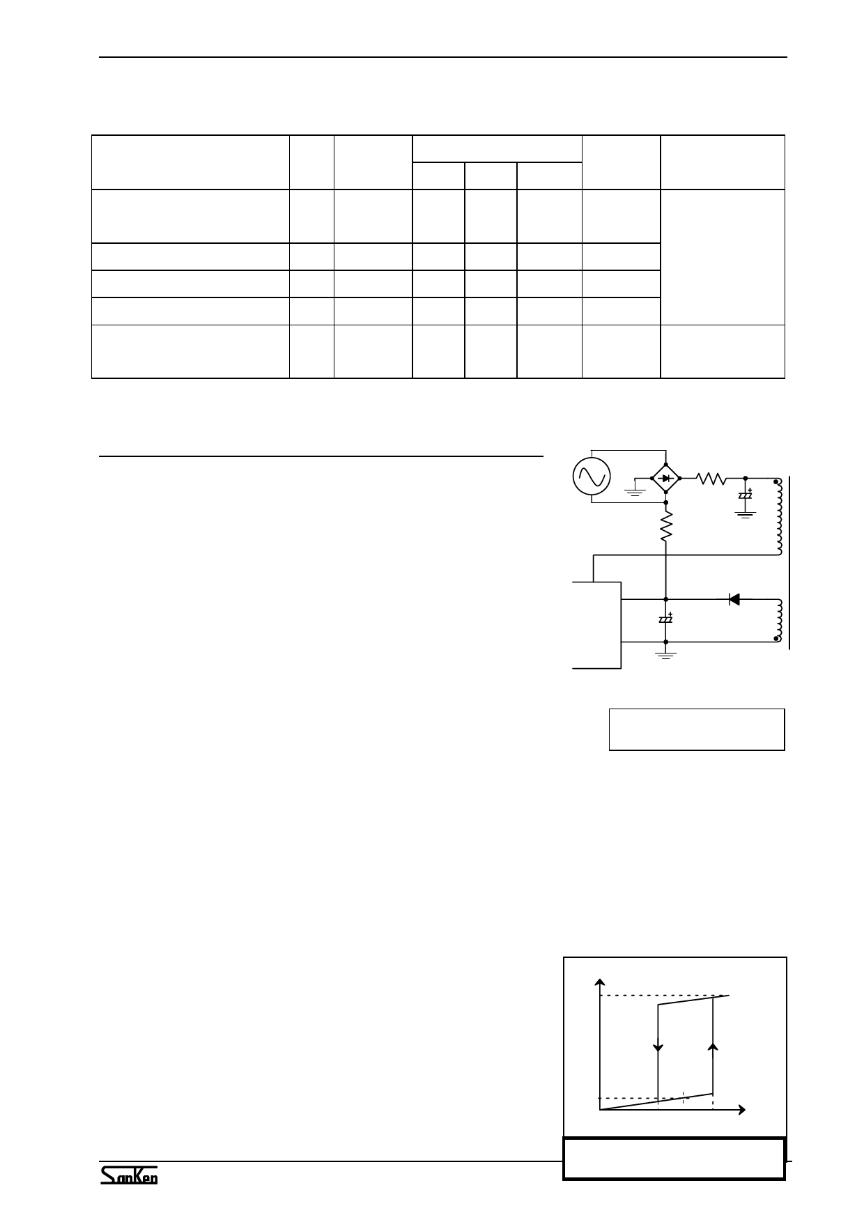
7.1 Vin Terminal(Pin 3)/Start-up Circuit
The start-up circuit detects the voltage at the VIN terminal (Pin 3), and
the circuit starts and stops the operation of the control IC. The power
supply circuit (VIN terminal input) of the control IC employs a circuit as
shown on Fig.1.
At start-up of the power supply, C2 is charged through the start-up
resistor Rs. The Rs value, due to the slight increase of the latch
circuit holding current (70uA MAX) at low temperature, should be
Rs
7,8
D3
VIN
C2
2,5
GND
determined in order for 100uA or higher current to flow at the minimum STR-A6300
P
D2
D
AC input voltage.
However, where the Rs value is too high, the current charging C2 after
図1 起動回路
Fig.1. Start-up Circuit
AC input shall be reduced, as a result, longer time is required to reach the operation start voltage.
Consequently, Rs value as well as C2 value that will be mentioned later should be monitored.
Vin terminal voltage falls immediately after the control circuit starts its operation, but the drop ratio of the
voltage shall reduce by increasing the C2 capacitance. Consequently, even though the start-up of the drive
winding voltage is delayed, the Vin terminal voltage would not reach the operation stop voltage to maintain
the start-up operation.
However, the time of AC input to operation start becomes longer since it takes much time to charge
the C2, if the C2 capacitance is too large. In general, a power supply shall operate at the value of
C2(=4.7~10uF approx.) and of Rs (=470kohm~1Mohm) for a wide IIN
input start-up.
5mA
(Max)
As shown on Fig.2, circuit current is kept below 50uA max.
(Vin=15.0V, Ta=25℃) until the control circuit starts its operation, and
a higher value of Rs is applicable to the circuit.
The control circuit starts its operation by start-up circuit as
soon as the Vin terminal voltage reaches 17.6V(TYP.), and the current
Page 8
50μA
(Max)
10.1V 15V
(typ)
19.4V
(Max)
VIN
図2 VIN 端子電圧-回路電流IIN
Fig.2. Vin-IIN(Circuit current)
Share Link: 