IXDP631 Ver la hoja de datos (PDF) - IXYS CORPORATION
Número de pieza
componentes Descripción
Fabricante
IXDP631 Datasheet PDF : 7 Pages
| |||
IXDP630
IXDP631
tendency to leave it off the schematic.
During the layout process, the engineer
must consider each and every connec-
tion from the standpoint of its contribu-
tion to system operation. How sensitive
is it? What noise producing lines are
routed near it? What transients can
occur between circuits tied to each end
of this trace...? With few exceptions,
modern autorouters cannot deal with
these requirements. If autorouters are
used, they produce layouts that will not
function.
Remember that the IXDP630/631 is the
interface between the control circuits
and the power circuits. Nowhere else
on the PCB are these problems more
likely to occur. Nowhere else will one
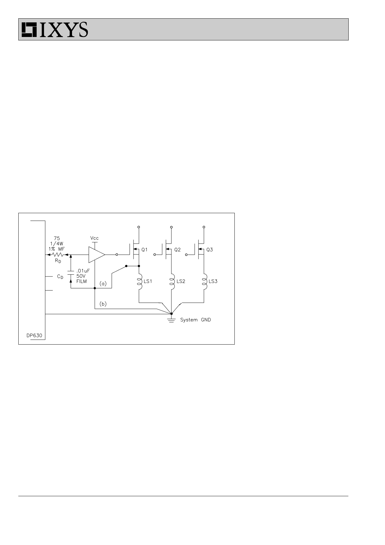
need to pay more attention. Fig. 7
illustrates an example layout problem.
The power circuit consists of three
the MOSFET is 6 V), the di/dt at turn-on
will be regulated by the driver/MOSFET/
LS1 loop to about 200 A/µs - quite a
surprise when your circuit requires
500 A/µs to operate correctly.
It is possible to make use of this beha-
vior to create a turn-on or turn-off di/dt
limiter (perhaps to snub the upper
freewheeling diode reverse recovery).
While possible, this is normally not
desirable or practical where two or
more transistors are controlled.
Equalizing the parasitic impedances of
three traces while positioning the
transistors next to their heat sink and
meeting UL/VDE voltage spacings is
just too difficult.
Grounding the gate drive buffer as in
option (a) solves the MOSFET turn on
problem by eliminating LS1 from the
Fig. 7. Potential layout problems that create functional problems.
power transistors (MOSFETs in this
example) controlled by a common
digital IC (the IXDP630). With the gate
drive amplifier (a discrete circuit or
possibly an IC driver like the
IXBD4410) grounded as in option (b),
the communication path from the
IXDP630 will operate without errors.
The PC trace induced voltages are not
common with the digital path so the
input of the gate drive buffer will not
see or respond to them. Unfortunately,
the MOSFET will not operate properly.
The voltage induced across LS1 when
Q1 is turned on, acts as source dege-
neration, modifying the turn-on behavior
of the MOSFET. If LS1 = 27 nH, and VCC
is 12 V (assuming the gate plateau of
I - 20
Source feedback loop. Now, unfortuna-
tely, the gate driver will oscillate every
time you turn it on or off. As the
IXDP630 output goes high, the gate
driver output follows (after its propaga-
tion delay) and the MOSFET starts to
conduct. The voltage transient induced
across LS1 (V = Ls1/di/dt) raises the
local ground (point a) until it exceeds
Voh (630)-Vil (gate buffer) and the buffer
(after its prop. delay) turns the MOSFET
off. Now the MOSFET current falls,
V(Ls1) drops, point (a) drops to (or
slightly below) system ground, and the
buffer detects a "1" at its input. After its
propagation delay, it again turns the
MOSFET on, continuing the oscillation
for one more cycle.
To eliminate this problem, a ground
level transformation circuit must be
added that rejects this common mode
transient. The simplest is a decoupling
circuit, also illustrated in Fig. 7. The
capacitor voltage (on Cd) remains
constant while the transient voltage is
dropped across Rd and the buffer
detects no input transition, eliminating
the oscillation. This circuit does add
significantly to turn-on and turn-off
delay time, and cannot be used if the
transient lasts as long as these delays
are allowed to extend. Delay times
must be considered in selection of
system deadtime.
It is also important to consider the
layout of the bypass capacitor as well
as the oscillator components in order to
keep these as close to the device as
possible.
Isolation
The most complex (and most effective)
method of eliminating the effects of
transients between grounds is isolation.
Optocouplers and pulse transformers
are the most commonly used isolation
techniques, and work very well in this
case. The IXDP630/631 has been
specifically designed to directly drive a
high speed optocoupler like the Hewlett
Packard HCPL22XX family or the
General Instrument 740L60XX
optologic family. These optos are
especially well suited to motor control
and power conversion equipment due
to their very high common-mode dv/dt
rejection capabilities.
The major problem associated with
using an optocoupler in a power circuit
is its common-mode dv/dt capability.
When a lower transistor is turned on, its
Collector (or Drain) is pulled to ground
very quickly. The optocoupler that
drives the upper transistor has its local
output stage referenced to the Emitter
(Source) of this upper device, which is
tied to the Collector of the lower device.
As this node moves, the dv/dt between
here and input circuit common is im-
pressed across the upper optocoupler.
This causes displacement currents to
flow in sensitive nodes in the optical
receiver circuitry, and may cause false
triggering of the output. Always pay
strict attention to the manufacturer's
recommended dv/dt ratings - exceeding
them could be disastrous.
© 1998 IXYS All rights reserved
Share Link: 