IXDP631 Ver la hoja de datos (PDF) - IXYS CORPORATION
Número de pieza
componentes Descripción
Fabricante
IXDP631 Datasheet PDF : 7 Pages
| |||
IXDP630
IXDP631
Application Information
Basic Operation
The IXDP630/631 Deadtime Genera-
tors are intended to simplify the
implementation of a single- or three-
phase digitally controlled power
conversion circuit. It replaces one to
three digital event counters (timer/
counters) in a microcontroller or DSP
implementation of a motor control, UPS
or other power system. In most cases
these timers are at a premium. They
must be used to calculate pulse width
on one to three independent modula-
tors, set interrupt service times, generate
a real-time clock, handle communica-
tions timing functions, etc.
The input command on the R, S and T
inputs is first synchronized with the
internal oscillator. When an input
changes state, the on output is
switched off, and after a deadtime of
exactly 8 clock periods, the complimen-
tary output is switched on. For exam-
ple, if input R is hi, output RU is hi. At
the first rising edge of CLK out after
input R is brought low, the RU output
goes low. After exactly 8 more clock
periods the RL output goes high. This
injected delay is the deadtime.
This method of synchronizing is utilized
to guarantee that the deadtime is
always exactly the same (to the accu-
racy of the CLK frequency). This can be
very important in certain applications.
Unbalanced deadtime creates an offset
in the PWM output stage transfer func-
tion, and can cause saturation of the
induction machine control or the driven
transformer if not corrected within a few
cycles.
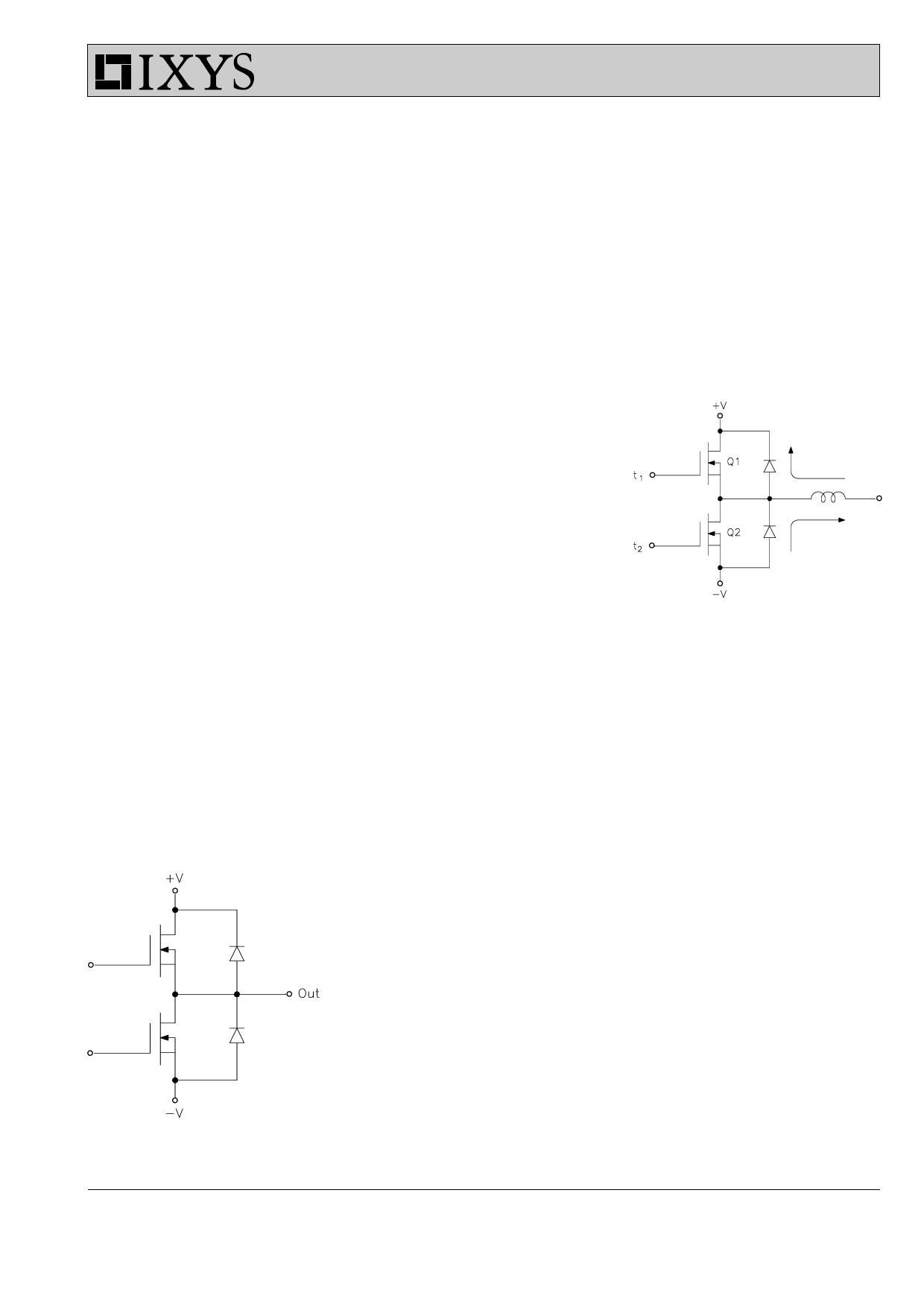
Fig. 1: Totem Pole configuration of
transistor switches; reason for dead-
time requirements
© 1998 IXYS All rights reserved
Deadtime in power circuits
Why is deadtime required?
Fig. 1 is typical of a switching power
conversion equipment output stage. It
has two (or typically more) switches. A
simple logic error - turning a transistor
on at the wrong instant - can cause
catastrophic failure in the right (or
wrong) circumstances.
In normal operation, when the state of
the output totem pole must change, the
conducting transistor is turned off.
Then, after a delay (usually called the
deadtime), the other transistor is turned
on. The delay is added to ensure that
there is no possibility of both transistors
conducting at the same time (this would
cause a short circuit of the DC link - a
"shoot through" - and would likely fail
both transistors in a few microseconds).
When the control logic commands a
switch to change to the off state,
several parasitics may delay/modify this
command. The propagation delay of
the control logic and gate drive buffer,
td (off) of the power transistor, storage
time (for bipolars) or tail time (for
IGBTs), voltage rise and current fall
times, etc., may be significant.
Problems Caused by Excessive
Deadtime
If a little is good, a lot should be better -
except with deadtime. Unfortunately,
deadband in the switching output stage
causes a nonlinearity in the power
circuit transfer function that may be
difficult for the control loop to remove.
Fig. 2 illustrates the problem. The
switching period T is:
T = t1 + t2 + DT
t1 is the time Q1 is commanded on, t2 is
the time Q2 is commanded on, and DT
is the deadtime. Assuming continuous
condition, and with current in the
direction of IL1:
thi = t1 + DT
tlo = t2
With current in the direction of IL2:
thi = t1 + DT
tlo = t2 + DT.
The change in "apparent duty cycle" is
then twice the deadtime (2DT). If
deadtime is 5% of the cycle period, the
duty cycle, as load current crosses
zero, instantly changes by 10 %. This is
a significant nonlinearity that causes
zero crossing distortions in load current
and voltage that must be removed by
the feedback loop around the PWM
stage. If these nonlinearities get large
enough, the loop may not have the gain
or the speed to remove them. This may
cause problems in the behavior of the
end product that are unacceptable.
Zero crossing distortion in the current of
a microstepped step motor, for examp-
le, causes very serious position errors,
velocity ripple, and audible noise in
operation - all undesirable.
IL1
IL2
Fig. 2: Problems caused by excessive
deadtime.
Calculating Appropriate Deadtime
Values
The designer must determine, under
worst case conditions, the absolute
maximum delay between the logic off
command and the actual cessation of
transistor conduction. This includes all
appropriate stages of logic, transistor
storage and delay times, etc. It is very
important to include special effects due
to the switch technology chosen.
Storage time of a bipolar transistor with
constant base drive can vary 10:1 as
collector current varies (storage time
increases dramatically at low collector
current, such as at light load). These
effects must be considered when
determining "worst case" delay time
requirements. A power circuit must not
only work at full rated load, but must
not fail under light or no load condi-
tions.
A delay of at least this time (plus a
guardband) must be injected in the
command to the series transistor so as
to absolutely prohibit its turn-on during
this interval.
I - 17
Share Link: 