2N6394TG Ver la hoja de datos (PDF) - ON Semiconductor
Número de pieza
componentes Descripción
Fabricante
2N6394TG Datasheet PDF : 6 Pages
| |||
2N6394 Series
Silicon Controlled Rectifiers
Reverse Blocking Thyristors
Designed primarily for half-wave ac control applications, such as
motor controls, heating controls and power supplies.
Features
• Glass Passivated Junctions with Center Gate Geometry for Greater
Parameter Uniformity and Stability
• Small, Rugged, Thermowatt Construction for Low Thermal
Resistance, High Heat Dissipation and Durability
• Blocking Voltage to 800 V
• These are Pb−Free Devices
MAXIMUM RATINGS † (TJ = 25°C unless otherwise noted)
Rating
Symbol Value
Unit
Peak Repetitive Off−State Voltage (Note 1) VDRM,
V
(TJ = −40 to 125°C, Sine Wave,
VRRM
50 to 60 Hz, Gate Open)
2N6394
50
2N6395
100
2N6397
400
2N6399
800
On-State RMS Current
IT(RMS)
12
A
(180° Conduction Angles; TC = 90°C)
Peak Non-Repetitive Surge Current
ITSM
100
A
(1/2 Cycle, Sine Wave, 60 Hz, TJ = 90°C)
Circuit Fusing (t = 8.3 ms)
I2t
40
A2s
Forward Peak Gate Power
(Pulse Width ≤ 1.0 ms, TC = 90°C)
PGM
20
W
Forward Average Gate Power
(t = 8.3 ms, TC = 90°C)
PG(AV)
0.5
W
Forward Peak Gate Current
(Pulse Width ≤ 1.0 ms, TC = 90°C)
IGM
2.0
A
Operating Junction Temperature Range
TJ −40 to +125 °C
Storage Temperature Range
Tstg −40 to +150 °C
MAXIMUM RATINGS † (TJ = 25°C unless otherwise noted)
Rating
Symbol
Max
Unit
Thermal Resistance, Junction−to−Case
RqJC
2.0
°C/W
Maximum Lead Temperature for Soldering
TL
Purposes 1/8″ from Case for 10 Seconds
260
°C
†Indicates JEDEC Registered Data
Stresses exceeding Maximum Ratings may damage the device. Maximum
Ratings are stress ratings only. Functional operation above the Recommended
Operating Conditions is not implied. Extended exposure to stresses above the
Recommended Operating Conditions may affect device reliability.
1. VDRM and VRRM for all types can be applied on a continuous basis. Ratings
apply for zero or negative gate voltage; however, positive gate voltage shall
not be applied concurrent with negative potential on the anode. Blocking
voltages shall not be tested with a constant current source such that the
voltage ratings of the devices are exceeded.
http://onsemi.com
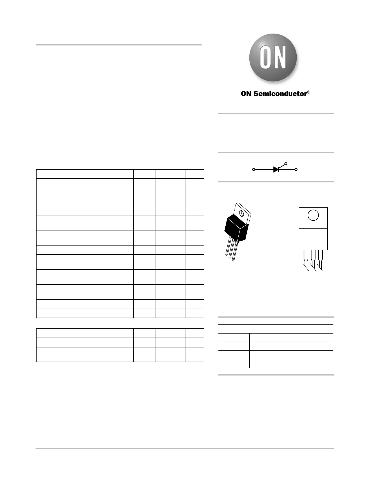
SCRs
12 AMPERES RMS
50 thru 800 VOLTS
G
A
K
MARKING
DIAGRAM
4
TO−220AB
CASE 221A
STYLE 3
2N639xG
AYWW
1
2
3
2N639x = Device Code
x = 4, 5, 7, or 9
G
= Pb−Free Package
A
= Assembly Location
Y
= Year
WW = Work Week
PIN ASSIGNMENT
1
Cathode
2
Anode
3
Gate
4
Anode
ORDERING INFORMATION
See detailed ordering and shipping information in the package
dimensions section on page 4 of this data sheet.
© Semiconductor Components Industries, LLC, 2012
1
September, 2012 − Rev. 9
Publication Order Number:
2N6394/D
Share Link: 