STU11N65M2(2019) Ver la hoja de datos (PDF) - STMicroelectronics
Número de pieza
componentes Descripción
Fabricante
STU11N65M2
(Rev.:2019)
(Rev.:2019)
STMicroelectronics

STU11N65M2 Datasheet PDF : 27 Pages
| |||
STD11N65M2, STP11N65M2, STU11N65M2
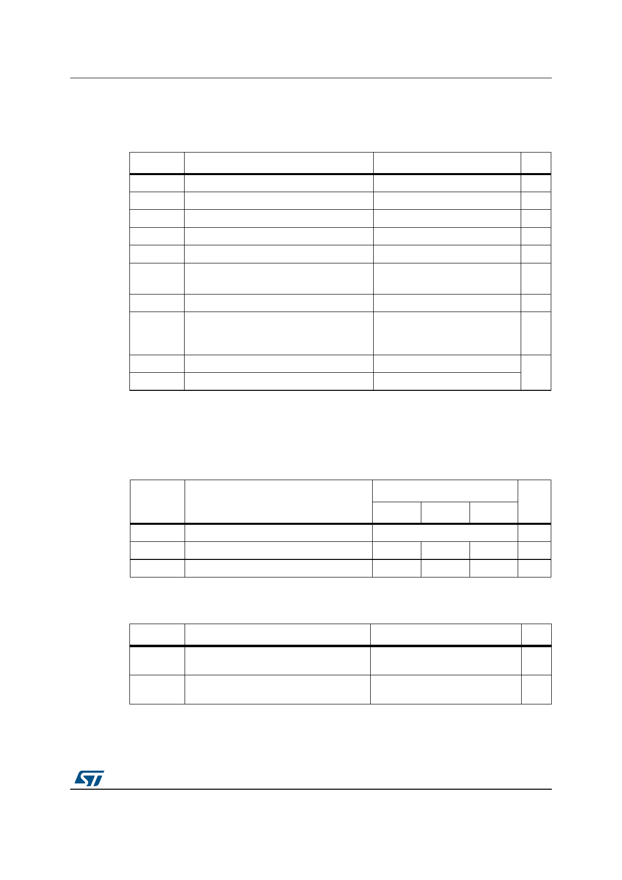
Electrical characteristics
2
Electrical characteristics
(Tcase = 25 °C unless otherwise specified)
Table 4. Static
Symbol Parameter
Test conditions
V(BR)DSS
Drain-source breakdown
voltage
VGS = 0 V, ID = 1 mA
IDSS
IGSS
VGS(th)
RDS(on)
Zero gate voltage drain
current
Gate-body leakage current
Gate threshold voltage
Static drain-source on-
resistance
VGS = 0 V, VDS = 650 V
VGS = 0 V, VDS = 650 V, Tcase = 125 °C(1)
VDS = 0 V, VGS = ±25 V
VDS = VGS, ID = 250 µA
VGS = 10 V, ID = 3.5 A
1. Defined by design, not subject to production test.
Min.
650
2
Typ.
3
0.60
Max.
1
100
±10
4
0.68
Unit
V
µA
µA
V
Ω
Table 5. Dynamic
Symbol Parameter
Test conditions
Min. Typ. Max. Unit
Ciss
Input capacitance
-
410
-
Coss
Output capacitance
VDS = 100 V, f = 1 MHz, VGS = 0 V
-
20
-
pF
Crss
Reverse transfer capacitance
-
0.9
-
Coss eq. (1) Equivalent output capacitance VDS = 0 to 520 V, VGS = 0 V
-
43
-
pF
RG
Intrinsic gate resistance
f = 1 MHz, ID = 0 A
-
6.4
-
Ω
Qg
Total gate charge
Qgs
Gate-source charge
Qgd
Gate-drain charge
VDD = 520 V, ID = 7 A, VGS = 0 to 10 V
(see Figure 16)
-
12.5
-
-
3.2
-
nC
-
5.8
-
1. Coss eq. is defined as a constant equivalent capacitance giving the same charging time as Coss when VDS increases from 0
to 80% VDSS.
Symbol
td(on)
tr
td(off)
tf
Parameter
Turn-on delay time
Rise time
Turn-off delay time
Fall time
Table 6. Switching times
Test conditions
Min. Typ. Max. Unit
-
9.5
-
VDD = 325 V, ID = 3.5 A RG = 4.7 Ω,
-
7.5
VGS = 10 V (see Figure 15 and Figure 20)
-
26
-
-
ns
-
15
-
DS10348 - Rev 6
page 3/27
Share Link: