NTE1549 Ver la hoja de datos (PDF) - NTE Electronics
Número de pieza
componentes Descripción
Fabricante
NTE1549 Datasheet PDF : 4 Pages
| |||
Absolute Maximum Ratings:
Power Dissipation (Note 1) . . . . . . . . . . . . . . . . . . . . . . . . . . . . . . . . . . . . . . . . . . . . . . . . . . . . . . . 625mW
Supply Voltage . . . . . . . . . . . . . . . . . . . . . . . . . . . . . . . . . . . . . . . . . . . . . . . . . . . . . . . . . . . . . . . . . . . . . 25V
Voltage on Output Drivers . . . . . . . . . . . . . . . . . . . . . . . . . . . . . . . . . . . . . . . . . . . . . . . . . . . . . . . . . . . 25V
Input Signal Overvoltage (Note 2) . . . . . . . . . . . . . . . . . . . . . . . . . . . . . . . . . . . . . . . . . . . . . . . . . . . ±35V
Divider Voltage . . . . . . . . . . . . . . . . . . . . . . . . . . . . . . . . . . . . . . . . . . . . . . . . . . . . . . . . . . . . –100mV to V+
Reference Load Current . . . . . . . . . . . . . . . . . . . . . . . . . . . . . . . . . . . . . . . . . . . . . . . . . . . . . . . . . . 10mA
Storage Temperature Range . . . . . . . . . . . . . . . . . . . . . . . . . . . . . . . . . . . . . . . . . . . . . . . –55° to +150°C
Lead Temperature (Soldering, 10 seconds) . . . . . . . . . . . . . . . . . . . . . . . . . . . . . . . . . . . . . . . . . +300°C
Note 1. The maximum junction temperature of the NTE1549 is 100°C. Devices must be derated for
operation at elevated temperatures. Junction to ambient thermal resistance is 120°C/W.
Note 2. Pin 5 input current must be limited to ±3mA. The addition of a 39k resistor in series with Pin5
allows ±100V signals without damage.
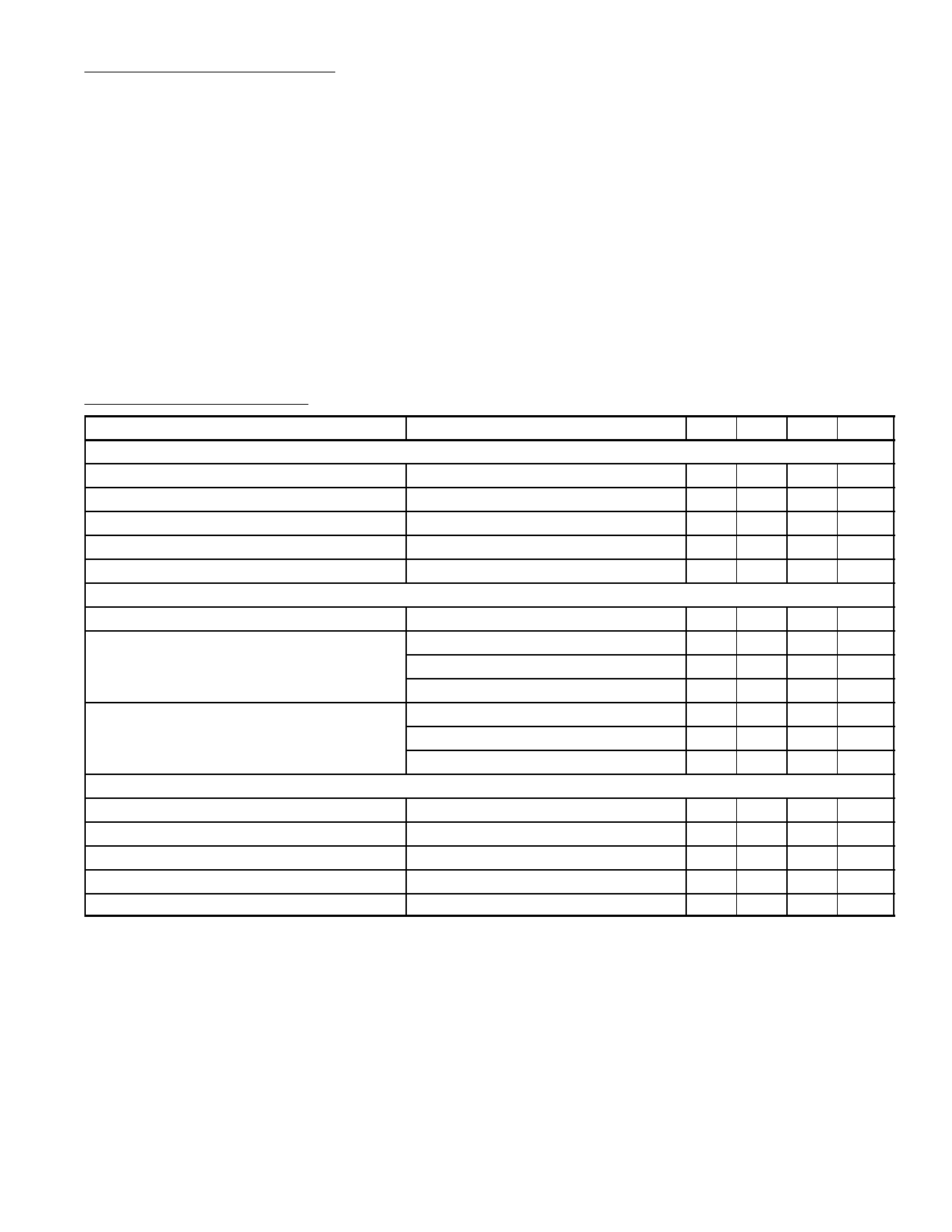
Electrical Characteristics: (Note 3)
Parameter
Comparators
Offset Voltage, Buffer and First Comparator
Offset Voltage, Buffer and Any Other Comparator
Gain (∆ILED/∆VIN)
Input Bias Current (At Pin5)
Input Signal Overvoltage
Voltage Divider
Divider Resistance
Relative Accuracy (Input Change Between Any Two
Threshold Points)
Absolute Accuracy
Voltage Reference
Output Voltage
Line Regulation
Load Regulation
Output Voltage Change with Temperature
Adjust Pin Current
Test Conditions
Min Typ Max Unit
0V ≤ VRLO = VRHI ≤ 12V, ILED = 1mA
0V ≤ VRLO = VRHI ≤ 12V, ILED = 1mA
I(REF) = 2mA, ILED = 10mA
0V ≤ VIN ≤ (V+ =1.5V)
No Change in Display
–
3
10
mV
–
3
15
mV
3
8
– mA/mV
–
25
100
nA
–35
–
+35
V
Total Pin6 to Pin4
–1dB ≤ VIN ≤ 3dB, Note 4
–7dB ≤ VIN ≤ –1dB, Note 4
–10dB ≤ VIN ≤ –7dB, Note 4
VIN = 2, 1, 0, –1dB
VIN = –3, –5dB
VIN = –7, –10, –20dB
8
12
17
kΩ
0.75 1.0 1.25
dB
1.5
2.0
2.5
dB
2.5
3.0
2.5
dB
–0.25
–
+0.25
dB
–0.5
–
+0.5
dB
–1
–
+1
dB
0.1mA ≤ IL(REF) ≤ 4mA, V+ = VLED = 5V
1.2 1.28 1.34
V
3V ≤ V+ ≤ 18V
–
0.01 0.03 %/V
0.1mA ≤ IL(REF) ≤ 4mA, V+ = VLED = 5V
–
0.4
2.0
%
0° ≤ TA ≤ +70°C, IL(REF) = 1mA, V+ = VLED = 5V –
1
–
%
–
75
120
mA
Note 3. Unless otherwise stated, all specifications apply with the following conditions:
3VDC ≤ V+ ≤ 20VDC; –0.015V ≤ VRLO ≤ 12VDC; TA = +25°C, IL(REF) = 0.2mA, Pin9 con-
nected to Pin3 bar mode.
3VDC ≤ VLED ≤ V+; VREF, VRHI, VRLO ≤ (V+ –1.5V); For higher power dissipations, pulse
testing is used.
–0.015V ≤ VRHI ≤ 12VDC; 0V ≤ VIN ≤ V+ –1.5V
Note 4. Accuracy is measured referred to +3dB = +3dB = +10.000VDC at Pin5, with +10.000VDC at
Pin6, and 0.000 VDC at Pin4. At lower full–scale voltages, buffer and comparator offset volt-
age may add significant error.
Share Link: 