IHLP1616BZER2R2M01 Ver la hoja de datos (PDF) - Vishay Semiconductors
NГәmero de pieza
componentes DescripciГіn
Fabricante
IHLP1616BZER2R2M01 Datasheet PDF : 5 Pages
| |||
www.vishay.com
IHLP-1616AB-01
Vishay Dale
Low Profile, High Current IHLPВ® Inductors
Manufactured under one or more of the following:пҖ
US Patents; 6,198,375/6,204,744/6,449,829/6,460,244.пҖ
Several foreign patents, and other patents pending.
STANDARD ELECTRICAL SPECIFICATIONS
L0
INDUCTANCE
HEAT
Вұ 20 % DCR DCR RATING SATURATION
AT 100 kHz, TYP. MAX. CURRENT CURRENT SRF
0.25 V, 0 A 25 В°C 25 В°C DC TYP. DC TYP. TYP.
(ОјH)
(mпҒ—) (mпҒ—) (A) (3)
(A) (4)
(MHz)
0.047
0.10
0.22
0.47
0.68
3.25 3.75 13.0
5.50 6.00 11.5
11.0 12.0
8.5
20.0 22.0
5.0
29.3 31.4
4.9
32.0
565
25.0
277
20.0
183
13.0
101
9.3
100
1.00
50.0 52.5
4.0
7.0
64
Notes
(1) All test data is referenced to 25 В°C ambient
(2) Operating temperature range -55 В°C to +125 В°C
(3) DC current (A) that will cause an approximate пҒ„T of 40 В°C
(4) DC current (A) that will cause L0 to drop approximately 20 %
(5) The part temperature (ambient + temp. rise) should not exceed
125 В°C under worst case operating conditions. Circuit design,
component placement, PWB trace size and thickness, airflow
and other cooling provisions all affect the part temperature. Part
temperature should be verified in the end application.
FEATURES
вҖў Shielded construction
вҖў Lowest DCR/ОјH, in this package size
вҖў Handles high transient current spikes without
saturation
вҖў Ultra low buzz noise, due to composite
construction
вҖў Excellent DC/DC energy storage up to 5 MHz.
Filter inductor applications up to SRF (see вҖңStandard
Electrical SpecificationsвҖқ table)
вҖў Material categorization: for definitions of compliance
please see www.vishay.com/doc?99912
APPLICATIONS
вҖў PDA / notebook / desktop / server applications
вҖў High current POL converters
вҖў Low profile, high current power supplies
вҖў Battery powered devices
вҖў DC/DC converters in distributed power systems
вҖў DC/DC converter for Field Programmable Gate Array
(FPGA)
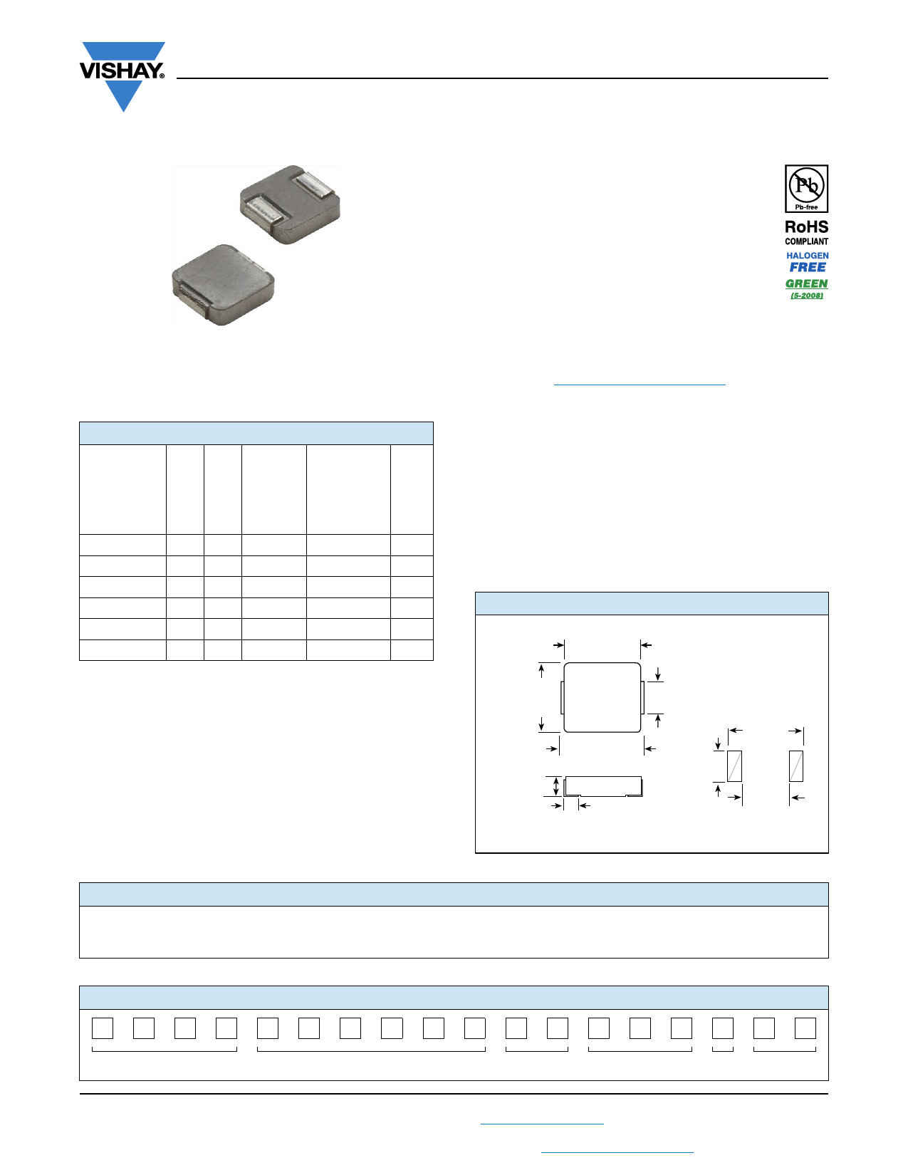
DIMENSIONS in inches [millimeters]
0.160 Вұ 0.010
[4.06 Вұ 0.254]
0.160 Вұ 0.010
[4.06 Вұ 0.254]
0.080 Вұ 0.002
[2.0 Вұ 0.05] Typical Pad Layout
0.175 Вұ 0.010
[4.45 Вұ 0.254]
0.047
[1.20]
Max.
0.030 Вұ 0.012
[0.76 Вұ 0.30]
0.090
[2.286]
0.222
[5.639]
0.076
[1.930]
DESCRIPTION
IHLP-1616AB-01
0.47 ОјH
MODEL
INDUCTANCE VALUE
Вұ 20 %
INDUCTANCE TOLERANCE
ER
e3
PACKAGE CODE JEDECВ® LEAD (Pb)-FREE STANDARD
GLOBAL PART NUMBER
I
H
L
P
1
6
1
6
A
B
E
R
R
4
7
M
0
1
PRODUCT FAMILY
SIZE
PACKAGE
CODE
INDUCTANCE
VALUE
TOL. SERIES
Revision: 15-Sep-16
1
Document Number: 34197
For technical questions, contact: magnetics@vishay.com
THIS DOCUMENT IS SUBJECT TO CHANGE WITHOUT NOTICE. THE PRODUCTS DESCRIBED HEREIN AND THIS DOCUMENT
ARE SUBJECT TO SPECIFIC DISCLAIMERS, SET FORTH AT www.vishay.com/doc?91000
Share Link: 