NTE2053 Ver la hoja de datos (PDF) - NTE Electronics
Número de pieza
componentes Descripción
Fabricante
NTE2053 Datasheet PDF : 5 Pages
| |||
Functional Description (Cont’d):
The converter is started by having CS and WR simultaneously low. This sets the start flip–flop (F/F)
and the resulting “1” level resets the 8–bit shift register, resets the interrupt (INTR) F/F and inputs a “1”
to the D flop, F/F1, which is at the input end of the 8–bit shift register. Internal clock signals then transfer
this “1” to the Q output of F/F1. The AND gate, G1, combines this “1” output with a clock signal to provide
a reset signal to the start F/F. If the set signal is no longer present (either WR or CS is a “1”) the start
F/F is reset and the 8–bit shift register then can have the “1” clocked in, which starts the conversion
process. If the set signal were to still be present, this reset pulse would have no effect (both outputs
of the start F/F would momentarily be at a “1” level) and the 8–bit shift register would continue to be held
in the reset mode. This logic therefore allows for wide CS and WR signals and the converter will start
after at least one of these signals returns high and the internal clocks again provide a reset signal for
the start F/F.
After the “1” is clocked through the 8–bit shift register (which completes the SAR search) it appears as
the input to the D–type latch, LATCH 1. As soon as this “1” is output from the shift register, the AND
gate, G2, causes the new digital word to transfer to the TRI–STATE output latches. When LATCH 1
is subsequently enabled, the Q output makes a high–to–low transition which causes the INTR F/F to
set. An inverting buffer then supplies the INTR input signal.
Note that the SET control of the INTR F/F remains low for 8 of the external clock periods (as the internal
clocks run at 1/8 of the frequency of the external clock). If the data output is continuously enabled (CS
and RD both are held low), the INTR output will still signal the end of conversion (by a high–to–low
transition), because the SET input can control the Q output of the INTR F/F even though the RESET
input is constant at a “1” level in this operating mode. This INTR output will therefore stay low for the
duration of the SET signal, which is 8 periods of the external clock frequency (assuming the A/D is
not started during this interval).
When operating in the free–running or continuous conversion mode (INTR pin tied to WR and CS wired
low), the START F/F is SET by the high–to–low transition of the INTR signal. This resets the SHIFT
REGISTER which causes the input to the D–type latch, LATCH 1, to go low. As the latch enable input
is still present, the Q output will go high, which then allows the INTR F/F to be RESET. This reduces
the width of the resulting INTR output pulse to only a few propagation delays (approximately 300ns).
When data is to be read, the combination of both CS and RD being low will cause the INTR F/F to be
reset and the TRI–STATE output latches will be enables to provide the 8–bit digital outputs.
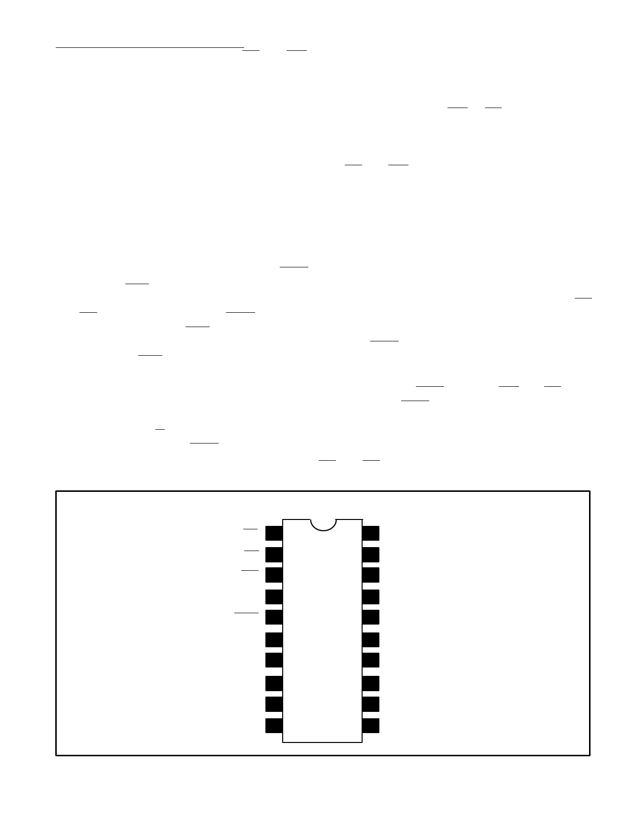
Pin Connection Diagram
CS 1
RD 2
WR 3
CLK IN 4
INTR 5
VIN (+) 6
VIN (–) 7
A GND 8
VREF/2 9
D GND 10
20 VCC
19 CLK R
18 DB0 (LSB)
17 DB1
16 DB2
15 DB3
14 DB4
13 DB5
12 DB6
11 DB7 (MSB)
Share Link: 