NTE2053 Ver la hoja de datos (PDF) - NTE Electronics
Número de pieza
componentes Descripción
Fabricante
NTE2053 Datasheet PDF : 5 Pages
| |||
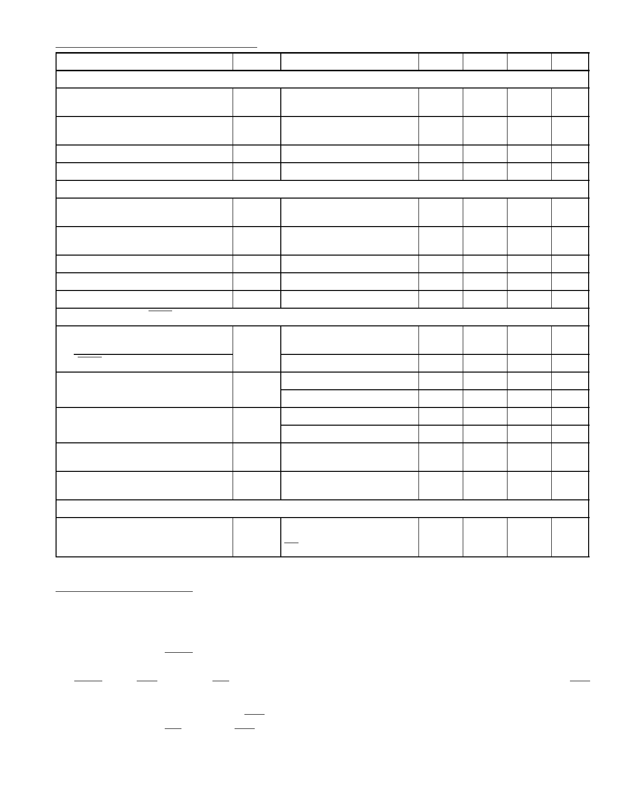
Electrical Characteristics (Cont’d): (VCC = 5V, TA = 0° to +70°C unless otherwise specified)
Parameter
Symbol
Test Conditions
Min
Typ
Max Unit
Control Inputs (Note: CLK IN (Pin4) is the input of a Schmitt trigger circuit and is therefore specified separately)
Logical “1” Input Voltage
(Except Pin4 CLK IN)
VIN(1) VCC = 5.25V
2.0
–
15
V
Logical “0” Input Voltage
(Except Pin4 CLK IN)
VIN(0) VCC = 4.75V
–
–
0.8
V
Logical “1” Input Current (All Inputs)
Logical “0” Input Current (All Inputs)
CLOCK IN and CLOCK R
IIN(1)
IIN(0)
VIN = 5V
VIN = 0V
–
0.005
1
µA
–1 –0.005
–
µA
CLK IN (Pin4) Positive Going
VT+
Threshold Voltage
2.7
3.1
3.5
V
CLK IN (Pin4) Negative Going
VT–
Threshold Voltage
1.5
1.8
2.1
V
CLK IN (Pin4) Hysteresis (VT+)–(VT–)
VH
0.6
1.3
2.0
V
Logical “0” CLK R Output Voltage
VOUT(0) VCC = 4.75V, IO = 360µA
–
–
0.4
V
Logical “1” CLK R Output Voltage
VOUT(1) VCC = 4.75V, IO = –360µA
2.4
–
–
V
Data Outputs and INTR
Logical “0” Output Voltage
Data Outputs
VOUT(0)
VCC = 4.75V, IOUT = 1.6mA
–
–
0.4
V
INTR Outputs
VCC = 4.75V, IOUT = 1.0mA
–
–
0.4
V
Logical “1” Output Voltage
VOUT(1) VCC = 4.75V, IO = –360µA
2.4
–
–
V
VCC = 4.75V, IO = –10µA
4.5
–
–
V
TRI–STATE Disable Output Leakage IOUT VOUT = 0V
(All Data Buffers)
VOUT = 5V
–3
–
–
–
–
µA
3
µA
Source Current
ISOURCE VOUT Short to GND,
TA = +25°C
4.5
6.0
–
mA
Sink Current
ISINK
VOUT Short to VCC,
TA = +25°C
9.0
16
–
mA
Power Supply
Supply Current (Includes Ladder
Current)
ICC fCLK = 640kHz,
–
1.1
1.8 mA
VREF/2 = NC. TA = +25°C,
CS = “1”
Functional Description:
The NTE2053 contains a circuit equivalent to the 256R network. Analog switches are sequenced by
successive approximation logic to match the analog difference input voltage [VIN(+) – VIN(–)] to a corre-
sponding tap on the R network. The most significant bit is tested first and after 8 comparisons (64 clock
cycles) a digital 8–bit binary code (1111 1111 = full–scale) is transferred to an output latch and then an
interrupt is asserted (INTR makes a high–to–low transition). A conversion in process can be interrupted
by issuing a second start command. The device may be operated in the free–running mode by connect-
ing INTR to the WR input with CS = 0. To insure start–up under all possible conditions, an external WR
pulse is required during the first power–up cycle.
On the high–to–low transition of the WR input the internal SAR latches and the shift register stages are
reset. As long as the CS input and WR input remain low. the A/D will remain in a reset state. Conversion
will start from 1 to 8 clock periods after at least one of these inputs makes a low–to–high transition.
Share Link: 