NTE2053 Ver la hoja de datos (PDF) - NTE Electronics
Número de pieza
componentes Descripción
Fabricante
NTE2053 Datasheet PDF : 5 Pages
| |||
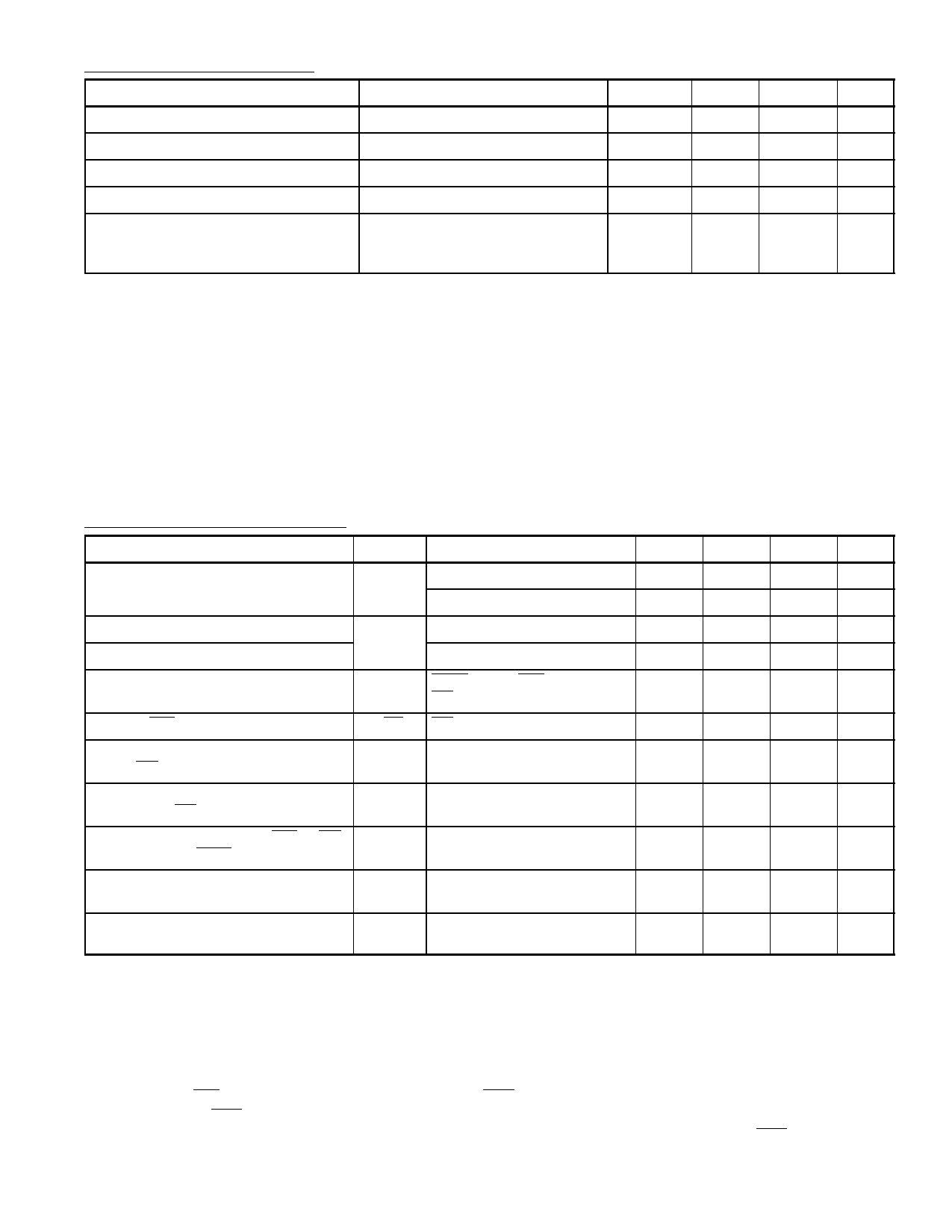
Electrical Characteristics: (VCC = 5V, TA = 0° to +70°C, fCLK = 640kHz unless otherwise specified)
Parameter
Test Conditions
Min
Typ
Max Unit
Total Unadjusted Error (Note 4)
VREF/2 = 2.500V
–
–
±1/2
LSB
VREF/2 Input Resistance
2.5
8.0
–
kΩ
Analog Input Voltage Range
DC Common–Mode Error
V(+) or V(–), Note 5
GND–0.05
Over Analog Input Voltage Range
–
–
±1/16
VCC+0.05 V
±1/8
LSB
Power Supply Sensitivity
VCC = 5V ±10% Over Allowed
VIN(+) and VIN(–) Voltage Range,
Note 5
±1/16
±1/8
LSB
Note 4. The NTE2053 A/D does not require a zero adjust.
Note 5. For VIN(–) ≥ VIN(+) the digital output code will be 0000 0000. Two on–chip diodes are tied
to each analog input which will forward conduct for analog input voltages one diode drop bel-
wo GND or one diode drop greater than the VCC supply. Be careful, during testing at low VCC
levels (4.5V), as high level analog inputs (5V) can cause this input diode to conduct – espe-
cially at elevated temperatures, and cause errors for analog inputs near full–scale. The spec
allows 50mV forward bias of either diode. This means that as long as the analog VIN does
not exceed the supply voltage by more than 50mV, the output code will be correct. To
achieve an absolute 0V to 5V input voltage range will therefore require a minimum supply
voltage of 4.950V over temperature variations, initial tolerance, and loading.
AC Electrical Characteristics: (VCC = 5V, TA = +25°C unless otherwise specified)
Parameter
Symbol
Test Conditions
Min
Typ
Conversion Time
TC fCLK = 640kHz, Note 7
Note 6, Note 7
103
–
66
–
Clock Frequency
Clock Duty Cycle
fCLK VCC = 5V, Note 6
Note 6
100
640
40
–
Conversion Rate in Free–Running
Mode
Width of WR Input (Start Pulse Width)
Access Time (Delay from Falling Edge
of RD to Output Data Valid)
CR
tW(WR)L
tACC
INTR tied to WR with
CS = 0V, fCLK = 640kHz
CS = 0, Note 8
CL = 100pF
–
–
100
–
–
135
TRI–STATE Control (Delay from Rising t1H, t0H CL = 10pF, RL = 10k
Edge of RD to Hi–Z State)
–
125
Delay from Falling Edge of WR or RD tWI, tRI
to Reset of INTR
–
300
Input Capacitance of Logic
CIN
Control Inputs
–
5
TRI–STATE Output Capacitance
(Data Buffers)
COUT
–
5
Max
114
73
1460
60
8770
Unit
µs
1/fCLK
kHz
%
conv/s
–
ns
200
ns
200
ns
450
ns
7.5
pF
7.5
pF
Note 6. Accuracy is guaranteed at fCLK = 640kHz. At higher clock frequencies accuracy can de-
grade. For lower clock frequencies, the duty cycle limits can be extended so long as the mini-
mum clock high time interval or minimum clock low time interval is no less than 275ns.
Note 7. With an asynchronous start pulse, up to 8 clock periods may be required before the internal
clock phases are proper to start the conversion process. The start request is internally
latched.
Note 8. The CS input is assumed to bracket the WR strobe input and therefore timing is dependent
on the WR pulse width. An arbitrary wide pulse width will hold the converter on a reset mode
and the start of conversion is initiated by the low to high transition of the WR pulse.
Share Link: 