LH543620M-30 Ver la hoja de datos (PDF) - Sharp Electronics
N√∫mero de pieza
componentes Descripción
Fabricante
LH543620M-30 Datasheet PDF : 38 Pages
| |||
LH543620
1024 √ó 36 Synchronous FIFO
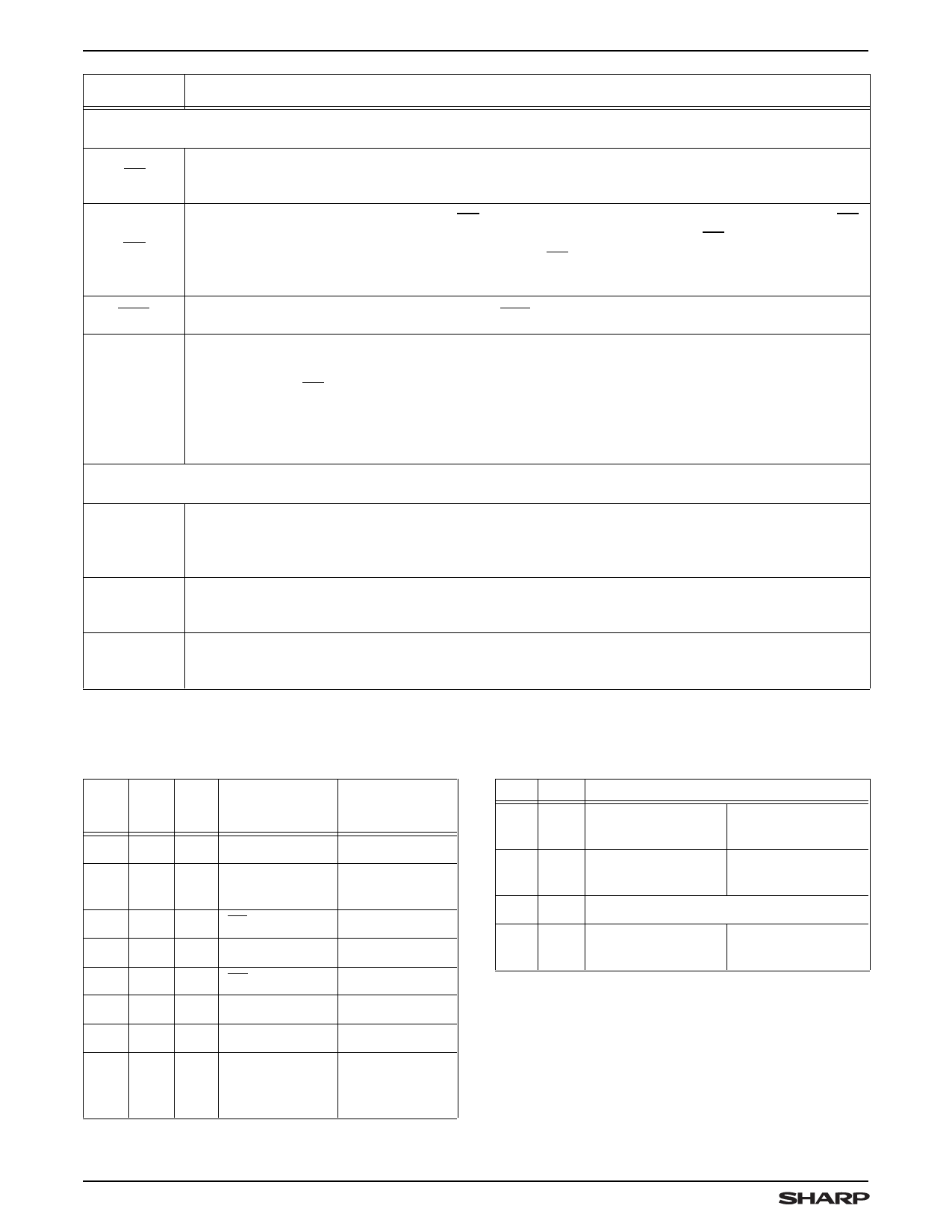
PIN NAME
DESCRIPTION
ASYNCHRONOUS CONTROL
RS
Master Reset. When asserted LOW, the LH543620 internal resource registers are set to their
default value. See Table 1. The status flags indicate Empty FIFO.
Output Enable. When asserted LOW, OE forces Q[35:0] to be active. When deasserted HIGH, OE
OE
forces Q[35:0] into a Hi-Z state. Bit 6 of the control register governs whether OE suppresses the
advancement of the Read Pointer (RP). In this case, OE must obey setup time and hold time
relative to CKO.
BYE
CAPR
Data-Bypass Enable. When asserted LOW, BYE connects Q[35:0] directly to D[35:0].
Command-Address Port Reference. CAPR determines the source of the 16-bit word to be loaded
into the resource register. Whenever CAPR is LOW, the word comes from the Input Port. Whenever
CAPR is HIGH (OE is HIGH), the word comes from the Output Port.
NOTES:
1. The destination of the resource register is always the Output Port.
2. CAPR is assumed to be a steady signal. It is not allowed to change ‘on-the-fly’ during operation.
CONTROL SIGNALS SYNCHRONOUS TO THE INPUT CLOCK
ENI1, ENI2
Input-Port Enables. ENI1 and ENI2 are active HIGH and synchronous to the rising edge of CKI.
Data is written into the FIFO memory array when both ENI1 and ENI2 are asserted HIGH.
NOTE: ENI1, ENI2 DO NOT ENABLE writing data into the Resource Registers or the Mailbox.
ADI[2:0]
Input-Port Address. ADI[2:0] specifies the Input-Port destination. See Table 1. ADI[2:0] is
synchronized to the rising edge of CKI.
WSI[1:0]
Input-Port Word-Width Selection. WSI[1:0] selects the Input-Port Word-Width. See Table 2.
WSI[1:0] is synchronous to the rising edge of CKI.
Table 1. Input-Port Address
ADI2 ADI1 ADI0
SELECTION
DEFAULT VALUE
(of the selected
REGISTER)
L L L RBASE register
0
L
L
H
ROFFSET
register
0
L H L AF offset value
8
L H H Parity register
0
H L L AE offset value
8
H L H Control register
1
H H L Mailbox
0
Resource
H H H registers write
disabled
Table 2. Input-Port Word-Width Selection
WSI1 WSI0
FUNCTION
L
L
9-Bit Data-Path
Width
Input data D[8:0]
L
H
18-Bit Data-Path
Width
Input data D[17:0]
H L Reserved
H
H
36-Bit Data-Path
Width
Input data D[35:0]
10
Share Link: 