XPT2046 Ver la hoja de datos (PDF) - Unspecified
Número de pieza
componentes Descripción
Fabricante
XPT2046 Datasheet PDF : 30 Pages
| |||
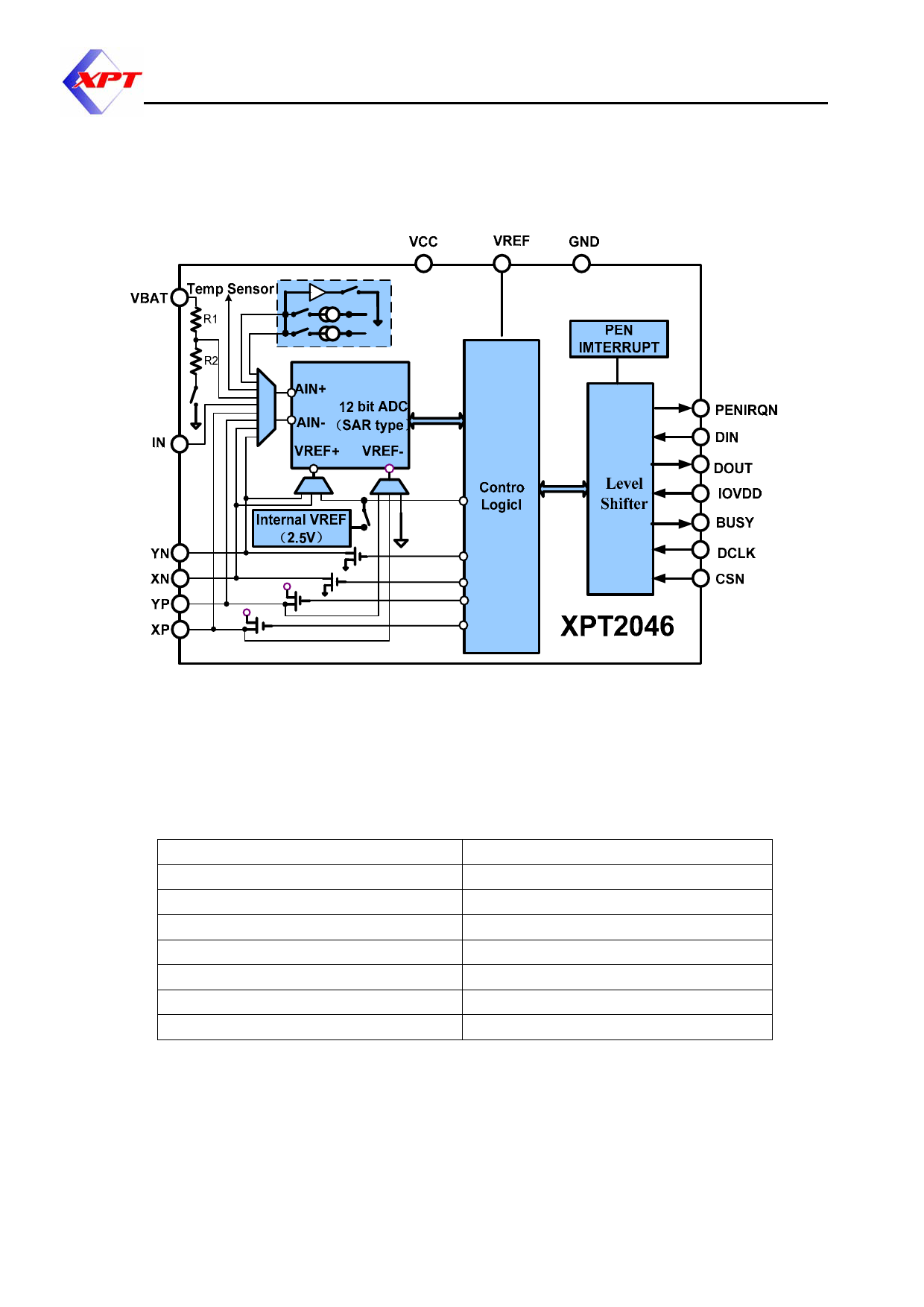
Block Diagram
XPT2046 Touch Screen Controller
Figure 1. Block Diagram
Absolute Maximum Ratings
+VCC and IOVDD to GND
Analog Inputs to GND
Digital Inputs to GND
Power Dissipation
Maximum Junction Temperature
Operating Temperature Range
Storage Temperature Range
Lead Temperature (soldering, 10s)
−0.3V to +6V
−0.3V to +VCC + 0.3V
−0.3V to IOVDD + 0.3V
. 250mW
+150°C
. −40°C to +85°C
−65°C to +150°C
+300°C
Table 1. Absolute Maximum Ratings
WARNING: Stresses above these ratings may cause permanent damage.Exposure to absolute maximum conditions
for xtended periods may degrade device reliability. These are stress ratings only, and functional operation of the
device at these or any other conditions beyond those specified is not implied.
Copyright©2007, SHENZHEN XPTEK TECHNOLOGY CO.,LTD http://www.xptek.com.cn
4/30
Share Link: 