RT9018A Ver la hoja de datos (PDF) - Richtek Technology
Número de pieza
componentes Descripción
Fabricante
RT9018A Datasheet PDF : 12 Pages
| |||
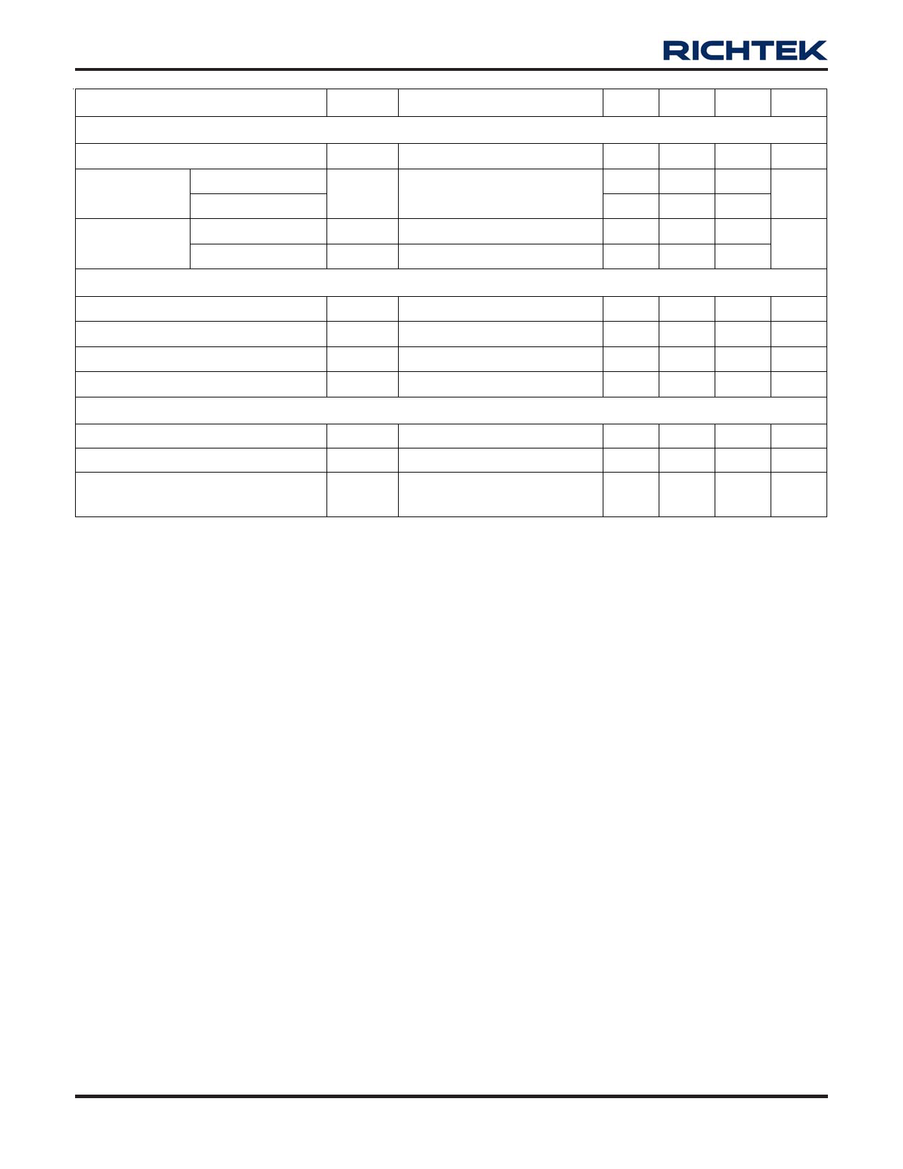
RT9018A/B
Parameter
Symbol
Test Conditions
Chip Enable
EN Input Bias Current
VDD Shutdown RT9018A
Current
RT9018B
IEN
ISHDN
VEN = 0V
VEN = 0V
EN Threshold
Power Good
Logic-Low Voltage VENL
Logic-High Voltage VENH
VDD = 5V
VDD = 5V
PGOOD Rising Threshold
PGOOD Hysteresis
PGOOD Sink Capability
PGOOD Delay
IPGOOD = 10mA
Thermal Protection
Thermal Shutdown Temperature
Thermal Shutdown Hysteresis
Thermal Shutdown Temperature
Fold-back
TSD
ΔTSD
VOUT < 0.4V
Min Typ Max Units
--
12
--
μA
--
10
20
μA
--
--
1
--
--
0.2
V
1.2
--
--
--
90
93
%
3
10
--
%
--
0.2 0.4
V
0.5 1.5
5
ms
--
160
--
°C
--
30
--
°C
--
110
--
°C
Note 1. Stresses listed as the above "Absolute Maximum Ratings" may cause permanent damage to the device. These are for
stress ratings. Functional operation of the device at these or any other conditions beyond those indicated in the
operational sections of the specifications is not implied. Exposure to absolute maximum rating conditions for extended
periods may remain possibility to affect device reliability.
Note 2. Devices are ESD sensitive. Handling precaution recommended.
Note 3. The device is not guaranteed to function outside its operating conditions.
Note 4. θJA is measured in the natural convection at TA = 25°C on a high effective thermal conductivity test board (4 Layers,
2S2P) of JEDEC 51-7 thermal measurement standard. The case point of θJC is on the expose pad for SOP-8 (Exposed
Pad) package.
Note 5. The dropout voltage is defined as VIN -VOUT, which is measured when VOUT is VOUT(NORMAL) - 100mV.
Note 6. Quiescent, or ground current, is the difference between input and output currents. It is defined by IQ = IIN - IOUT under no
load condition (IOUT = 0mA). The total current drawn from the supply is the sum of the load current plus the ground pin
current.
Note 7. Regulation is measured at constant junction temperature by using a 2ms current pulse. Devices are tested for load
regulation in the load range from 1mA to 3A.
www.richtek.com
4
DS9018A/B-04 September 2007
Share Link: 