AD588AQ(RevD) Ver la hoja de datos (PDF) - Analog Devices
Número de pieza
componentes Descripción
Fabricante
AD588AQ Datasheet PDF : 16 Pages
| |||
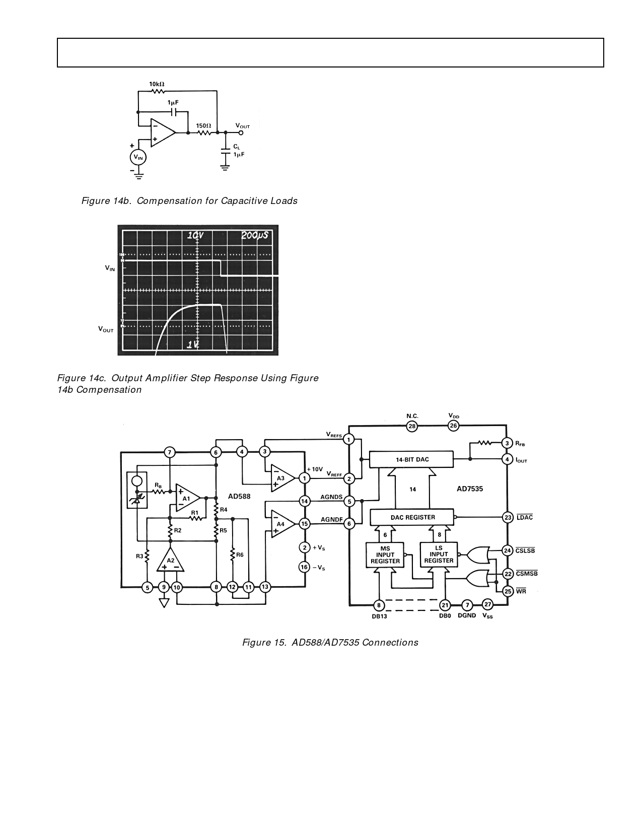
AD588
Figure 15b. Large-Scale Transient Response
Figures 16a and 16b display the output amplifier characteristics
driving a 5 mA to 10 mA load, a common situation found when
the reference is shared among multiple converters or is used to
provide a bipolar offset current.
A3 OR A4
+
10V
–
IL 2k⍀
VOUT
2k⍀
VL
10V
0V
Figure 16a. Transient and Constant Load Test Circuit
Figure 17b. Output Response with Capacitive Load
Figures 18a and 18b display the crosstalk between output am-
plifiers. The top trace shows the output of A4, dc-coupled and
offset by 10 V, while the output of A3 is subjected to a 0 mA
to 10 mA load current step. The transient at A4 settles in about
1 µs, and the load-induced offset is about 100 µV.
A4
+
10V
–
VOUT
VL
A3
1k⍀
10V
0V
+
10V
–
Figure 18a. Load Crosstalk Test Circuit
Figure 16b. Transient Response 5 mA to10 mA Load
In some applications, a varying load may be both resistive and
capacitive in nature or be connected to the AD588 by a long
capacitive cable.
Figures 17a and 17b display the output amplifier characteristics
driving a 1,000 pF, 0 mA to 10 mA load.
A3 OR A4
VOUT
1000pF
1k⍀
10V
CL
VL
10V
0V
Figure 17a. Capacitive Load Transient Response
Test Circuit
REV. D
–9–
Figure 18b. Load Crosstalk
Share Link: 