LR1102L Ver la hoja de datos (PDF) - Unisonic Technologies
Número de pieza
componentes Descripción
Fabricante
LR1102L Datasheet PDF : 12 Pages
| |||
LR1102
CMOS IC
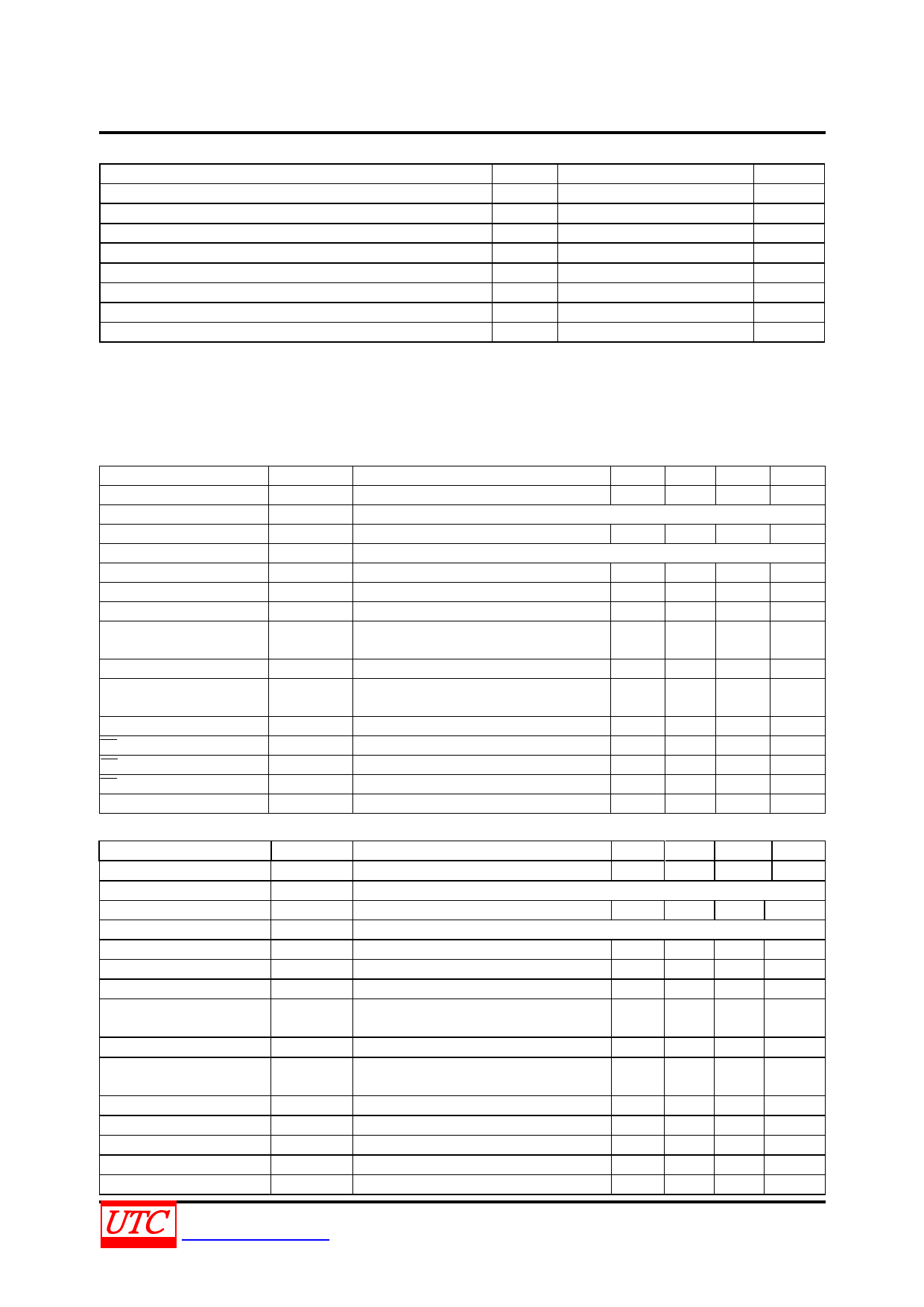
ABSOLUTE MAXIMUM RATING
PARAMETER
SYMBOL
RATINGS
UNIT
Input Voltage
VIN
9
V
Input Voltage
VCE
-0.3 ~ VIN+0.3
V
Output Voltage
VOUT
-0.3 ~ VIN+0.3
V
Output Current
IOUT
200
mA
Power Dissipation
PD
250
mW
Junction Temperature
TJ
+125
℃
Operating Temperature
TOPR
-20 ~ +85
℃
Storage Temperature
TSTG
-40 ~ +150
℃
Note1.Absolute maximum ratings are those values beyond which the device could be permanently damaged.
Absolute maximum ratings are stress ratings only and functional device operation is not implied.
2.The device is guaranteed to meet performance specification within 0℃~+70℃ operating temperature range
and assured by design from -20℃~+85℃.
ELECTRICAL CHARACTERISTICS
LR1102A-XX (TOPR=25℃)
PARAMETER
SYMBOL
TEST CONDITIONS
MIN TYP MAX UNIT
Output Voltage
Output Current
Load Regulation
Dropout Voltage
Supply Current
Supply Current (Standby)
Line Regulation
Ripple Rejection
Input Voltage
Output Voltage
Temperature Coefficient
Short Current Limit
CE Pull-up Resistance
CE Input Voltage ”H”
CE Input Voltage ”L”
Output Noise
VOUT VIN=Set VOUT + 1V, 1mA≤IOUT≤30mA
VOUTx0.98
IOUT Refer to the Electrical Characteristics by Output Voltage
∆VOUT/∆IOUT VIN=Set VOUT + 1V, 1mA≤IOUT≤80mA
12
VDIF Refer to the Electrical Characteristics by Output Voltage
ISS
VIN=Set VOUT + 1V
10
IST-BY VIN=VCE=Set VOUT + 1V
0.1
∆VOUT/∆VIN Set VOUT + 0.5V≤VIN≤8V, IOUT=30mA
0.05
f=1kHz, Ripple 0.5Vp-p
RR
70
VIN=Set VOUT+ 1V
VIN
2
∆VOUT/∆T IOUT = 30mA, -20℃≤TOPR≤85℃
±100
ILIMIT
RPU
VCEH
VCEL
eN
VOUT=0V
BW = 10Hz ~ 100kHz
200
2.5 5.0
1.5
0.00
30
VOUTx1.02
V
40
mV
20
µA
1.0
µA
0.20 %/V
dB
8
V
ppm/℃
10.0
VIN
0.25
mA
MΩ
V
V
µVrms
LR1102B-XX (TOPR=25℃)
PARAMETER
SYMBOL
TEST CONDITIONS
MIN TYP MAX UNIT
Output Voltage
Output Current
Load Regulation
Dropout Voltage
Supply Current
Supply Current (Standby)
Line Regulation
Ripple Rejection
Input Voltage
Output Voltage
Temperature Coefficient
VOUT VIN=Set VOUT + 1V, 1mA≤IOUT≤30mA
VOUTx0.98
IOUT Refer to the Electrical Characteristics by Output Voltage
∆VOUT/∆IOUT VIN=Set VOUT + 1V, 1mA≤IOUT≤80mA
12
VDIF Refer to the Electrical Characteristics by Output Voltage
ISS
VIN=Set VOUT + 1V
10
IST-BY VIN= Set VOUT + 1V, VCE=GND
0.1
∆VOUT/∆VIN Set VOUT + 0.5V≤VIN≤8V, IOUT=30mA
0.05
f=1kHz, Ripple 0.5Vp-p
RR
70
VIN=Set VOUT + 1V
VIN
2
∆VOUT/∆T IOUT = 30mA, -20℃≤TOPR≤85℃
±100
VOUTx1.02
V
40
mV
20
µA
1.0
µA
0.20 %/V
dB
8
V
ppm/℃
Short Current Limit
CE Pull-down Resistance
CE Input Voltage ”H”
CE Input Voltage ”L”
Output Noise
ILIMIT
RPD
VCEH
VCEL
eN
VOUT=0V
BW = 10Hz ~ 100kHz
200
mA
2.5 5.0 10.0 MΩ
1.5
VIN
V
0.00
0.25
V
30
µVrms
UNISONIC TECHNOLOGIES CO., LTD
www.unisonic.com.tw
4 of 12
QW-R502-038,C
Share Link: 