SZSMF12CT1G Ver la hoja de datos (PDF) - ON Semiconductor
Número de pieza
componentes Descripción
Fabricante
SZSMF12CT1G Datasheet PDF : 6 Pages
| |||
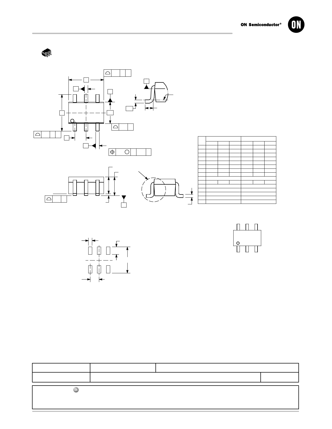
MECHANICAL CASE OUTLINE
PACKAGE DIMENSIONS
1
SCALE 2:1
E
2X
bbb H D
e
6X
ccc C
SC−88/SC70−6/SOT−363
CASE 419B−02
ISSUE Y
2X
DATE 11 DEC 2012
aaa H D
D
A
D
6
54
L2
E1
1
23
aaa C
2X 3 TIPS
H
L
DETAIL A
GAGE
PLANE
NOTES:
1. DIMENSIONING AND TOLERANCING PER ASME Y14.5M, 1994.
2. CONTROLLING DIMENSION: MILLIMETERS.
3. DIMENSIONS D AND E1 DO NOT INCLUDE MOLD FLASH,
PROTRUSIONS, OR GATE BURRS. MOLD FLASH, PROTRU-
SIONS, OR GATE BURRS SHALL NOT EXCEED 0.20 PER END.
4. DIMENSIONS D AND E1 AT THE OUTERMOST EXTREMES OF
THE PLASTIC BODY AND DATUM H.
5. DATUMS A AND B ARE DETERMINED AT DATUM H.
6. DIMENSIONS b AND c APPLY TO THE FLAT SECTION OF THE
LEAD BETWEEN 0.08 AND 0.15 FROM THE TIP.
7. DIMENSION b DOES NOT INCLUDE DAMBAR PROTRUSION.
ALLOWABLE DAMBAR PROTRUSION SHALL BE 0.08 TOTAL IN
EXCESS OF DIMENSION b AT MAXIMUM MATERIAL CONDI-
TION. THE DAMBAR CANNOT BE LOCATED ON THE LOWER
RADIUS OF THE FOOT.
B
TOP VIEW
6X b
ddd M C A-B D
A2
A
DETAIL A
A1
SIDE VIEW
C
SEATING
PLANE
c
END VIEW
MILLIMETERS
INCHES
DIM MIN NOM MAX MIN NOM MAX
A −−− −−− 1.10 −−− −−− 0.043
A1 0.00 −−− 0.10 0.000 −−− 0.004
A2 0.70 0.90 1.00 0.027 0.035 0.039
b 0.15 0.20 0.25 0.006 0.008 0.010
C 0.08 0.15 0.22 0.003 0.006 0.009
D 1.80 2.00 2.20 0.070 0.078 0.086
E 2.00 2.10 2.20 0.078 0.082 0.086
E1 1.15 1.25 1.35 0.045 0.049 0.053
e
0.65 BSC
0.026 BSC
L 0.26 0.36 0.46 0.010 0.014 0.018
L2
0.15 BSC
0.006 BSC
aaa
0.15
0.006
bbb
0.30
0.012
ccc
0.10
0.004
ddd
0.10
0.004
GENERIC
MARKING DIAGRAM*
RECOMMENDED
6
SOLDERING FOOTPRINT*
6X
0.30
6X
0.66
XXXMG
G
1
2.50
0.65
PITCH
DIMENSIONS: MILLIMETERS
*For additional information on our Pb−Free strategy and soldering
details, please download the ON Semiconductor Soldering and
Mounting Techniques Reference Manual, SOLDERRM/D.
XXX = Specific Device Code
M = Date Code*
G = Pb−Free Package
(Note: Microdot may be in either location)
*Date Code orientation and/or position may
vary depending upon manufacturing location.
*This information is generic. Please refer to
device data sheet for actual part marking.
Pb−Free indicator, “G” or microdot “ G”,
may or may not be present.
STYLES ON PAGE 2
DOCUMENT NUMBER: 98ASB42985B
DESCRIPTION: SC−88/SC70−6/SOT−363
Electronic versions are uncontrolled except when accessed directly from the Document Repository.
Printed versions are uncontrolled except when stamped “CONTROLLED COPY” in red.
PAGE 1 OF 2
ON Semiconductor and
are trademarks of Semiconductor Components Industries, LLC dba ON Semiconductor or its subsidiaries in the United States and/or other countries.
ON Semiconductor reserves the right to make changes without further notice to any products herein. ON Semiconductor makes no warranty, representation or guarantee regarding
the suitability of its products for any particular purpose, nor does ON Semiconductor assume any liability arising out of the application or use of any product or circuit, and specifically
disclaims any and all liability, including without limitation special, consequential or incidental damages. ON Semiconductor does not convey any license under its patent rights nor the
rights of others.
© Semiconductor Components Industries, LLC, 2019
www.onsemi.com
Share Link: 