MAX3543 Ver la hoja de datos (PDF) - Maxim Integrated
Número de pieza
componentes Descripción
Fabricante
MAX3543 Datasheet PDF : 20 Pages
| |||
Multiband Analog and
Digital Television Tuner
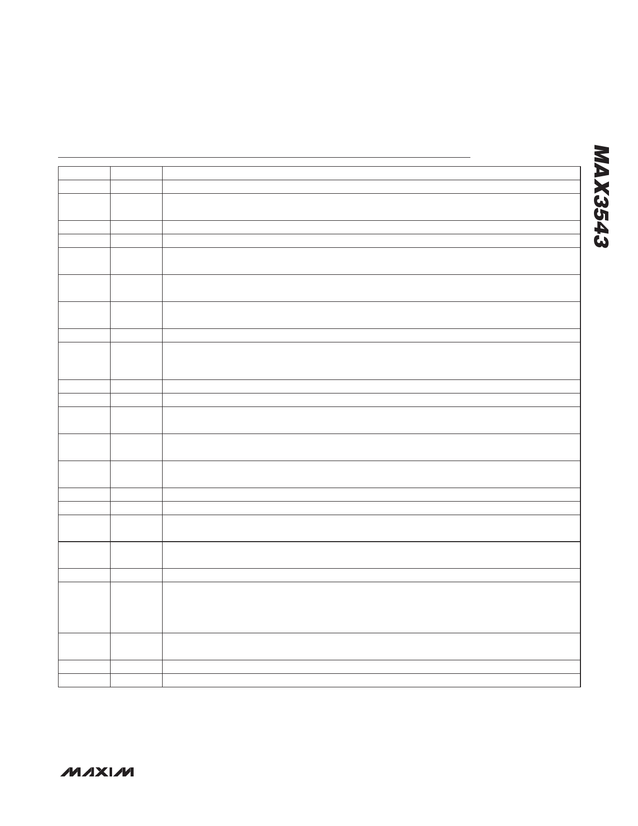
Pin Description
PIN
NAME
FUNCTION
1
RFINH High-Frequency RF Input. Matched to 75I over the operating band. Requires a DC-blocking capacitor.
2
RFGND1
RF Ground. Bypass to the PCB’s ground plane with a 1000pF capacitor. Keep traces as short as
possible to minimize inductance to ground plane. Do not connect RFGND1 and RFGND2 together.
3
RFVGC RF VGA Gain Control Voltage. Accepts a DC voltage from 0.5V to 3V.
4
VCCIF IF Power Supply. Requires a 600I series ferrite bead to a bypass capacitor to ground.
5
RFGND2
RF Ground. Bypass to the PCB’s ground plane with a 1000pF capacitor. Keep traces as short as
possible to minimize inductance to ground plane. Do not connect RFGND1 and RFGND2 together.
6
IFOUT1A
Dual-Mode DTV IF Output. In single-ended mode, this pin is the IF signal output. In differential mode, this
pin is the positive terminal of the differential IF output.
7
IFOUT1B
Dual-Mode DTV IF Output. In single-ended mode, this pin is the SAW filter bandwidth switch. In
differential mode, this pin is the negative terminal of the differential IF output.
8
IFVGC IF VGA Gain Control Voltage. Accepts a DC voltage from 0.5V to 3V.
2-Wire Serial-Interface Address Line. This pin sets the device address for the I2C-compatible serial
9
ADDR interface. There are three selectable addresses based on the state of this pin: logic-low, logic-high, or
unconnected.
10, 11 IFIN-, IFIN+ Differential IF VGA Input. Connect to the IF filter output.
12, 17, 26 GND Ground. Connect pin to paddle ground to minimize trace inductance.
13, 27,
29, 39
VCC Power-Supply Connections. Bypass each supply pin with a separate 1000pF capacitor to ground.
14
IFOUT2
Single-Ended IF Output. Connect to the analog demodulator input. Requires a 1000pF DC-blocking
capacitor.
15, 16
DTVOUT-,
DTVOUT+
Differential IF VGA Output. Connect to the demodulator input. Requires a 1000pF DC-blocking capacitor.
18
REFOUT Crystal Output to Drive Baseband IC. Output frequency is fXTAL or fXTAL/4.
19
VCCDIG Digital Supply. Requires a 15I series resistor to a 1FF bypass capacitor.
20
SCL
2-Wire Serial Clock Interface. Connect to the serial bus and ensure the bus includes an approximately
5kI pullup resistor.
21
XTALB
Crystal Oscillator Base. Connect to the crystal through a DC-blocking capacitor and connect a capacitor
to XTALE.
22
XTALE Crystal Oscillator Emitter. Connect a capacitor to ground and a capacitor to XTALB.
Reference Frequency Divider Control. Three modes are available depending on the state of this pin:
23
REFDIV
high = fXTAL/1, low = fXTAL/4, unconnected = state determined by register. Note: Power-up state of
register is not guaranteed; therefore, unconnected mode should only be used if the controller can
reprogram I2C in any of the divider settings.
24
SDA
2-Wire Serial Data Interface. Connect to serial bus and ensure the bus includes an approximately 5kI
pullup resistor.
25
TUNE PLL Charge-Pump Output and TUNE Input. Connect to the PLL loop filter.
28
LDOBYP Bypass for On-Chip VCO LDO. Bypass to ground with a 0.47FF capacitor.
_______________________________________________________________________________________ 7
Share Link: 