MAX8863 Ver la hoja de datos (PDF) - ON Semiconductor
Número de pieza
componentes Descripción
Fabricante
MAX8863 Datasheet PDF : 12 Pages
| |||
MAX8863
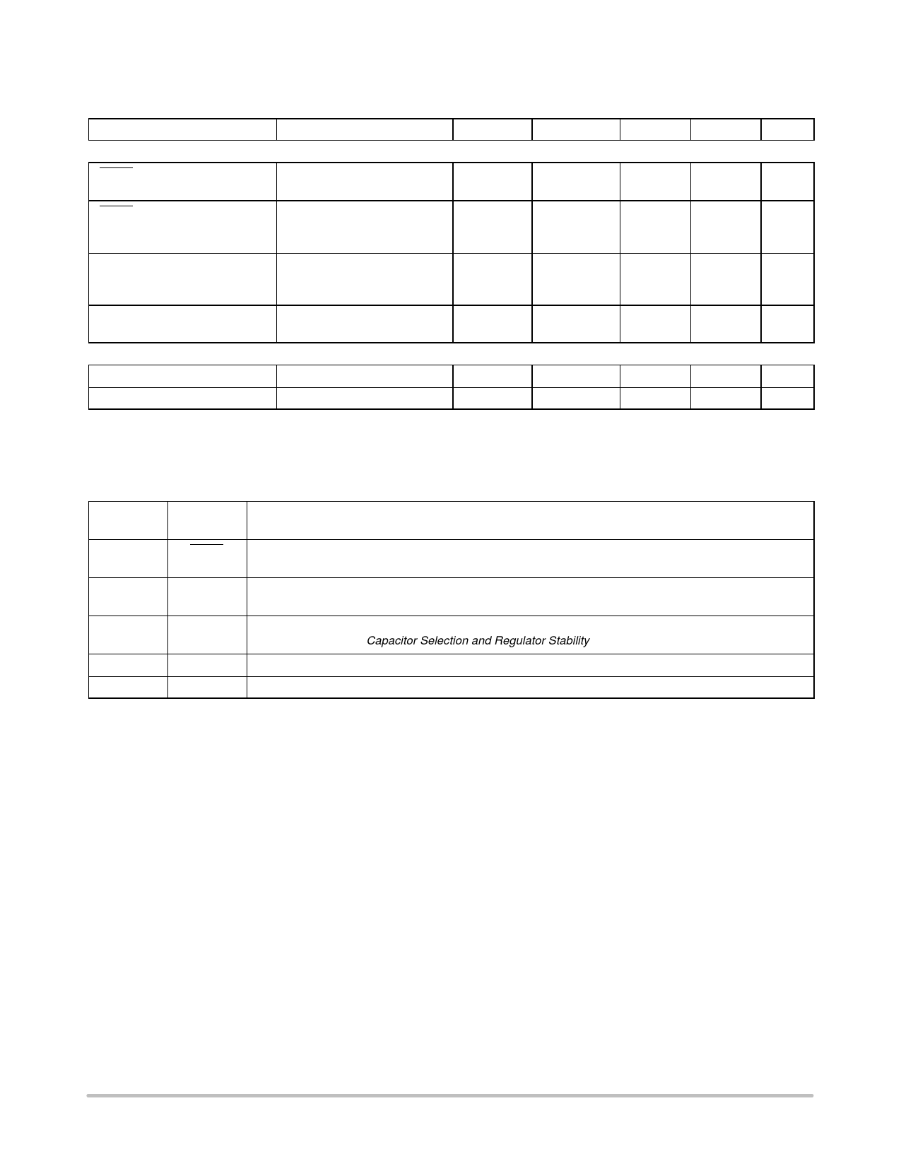
ELECTRICAL CHARACTERISTICS (continued) (VIN = +3.6 V, GND = 0 V, TA = TMIN to TMAX, unless otherwise specified.
Typical values are at TA = +25°C.) (Note 7.)
Characteristics
Test Conditions
Symbol
Min
Typ
Max
Unit
Shutdown
SHDN Input Threshold
–
VIH
2.0
–
–
V
VIL
–
–
0.4
SHDN Input Bias Current
Shutdown Supply Current
Shutdown to Output
Discharge Delay
VSHDN = VIN
TA = +25°C
TA = TMAX
ISHDN
–
–
VOUT = 0 V
TA = +25°C
TA = TMAX
IQSHDN
–
–
COUT = 1.0 µF, No Load
–
–
to 10% of VOUT
nA
0
100
50
–
µA
.002
1.0
0.02
–
1.0
–
msec
Thermal Protection
Thermal Shutdown Temperature
–
TSHDN
–
170
–
°C
Thermal Shutdown Hysteresis
–
DTSHDN
–
20
–
°C
7. Limits are 100% production tested at TA = +25°C. Limits over the operating temperature range are guaranteed through correlation using
Statistical Quality Control (SQC) Methods.
PIN DESCRIPTION
Pin
Number
Symbol
1
SHDN
2
GND
3
IN
4
OUT
5
GND
Description
Active–Low Shutdown Input. A logic low reduces the supply current to 0.1 nA. A logic low also causes
the output voltage to discharge to GND. Connect to IN for normal operation.
Ground. This pin also functions as a heatsink. Solder to large pads or the circuit board ground plane to
maximize thermal dissipation.
Regulator Input. Supply voltage can range from +2.5 V (+2.7 V for VOUT = 1.8 V) to +6.0 V. Bypass with
1.0 µF to GND (see Capacitor Selection and Regulator Stability).
Regulator Output. Sources up to 120 mA. Bypass with a 1.0 µF, t 1.0 Ω typical ESR capacitor to GND.
Connect to GND.
http://onsemi.com
3
Share Link: 