UDA1334ATS Ver la hoja de datos (PDF) - NXP Semiconductors.
Número de pieza
componentes Descripción
Fabricante
UDA1334ATS Datasheet PDF : 22 Pages
| |||
NXP Semiconductors
Low power audio DAC with PLL
Product specification
UDA1334ATS
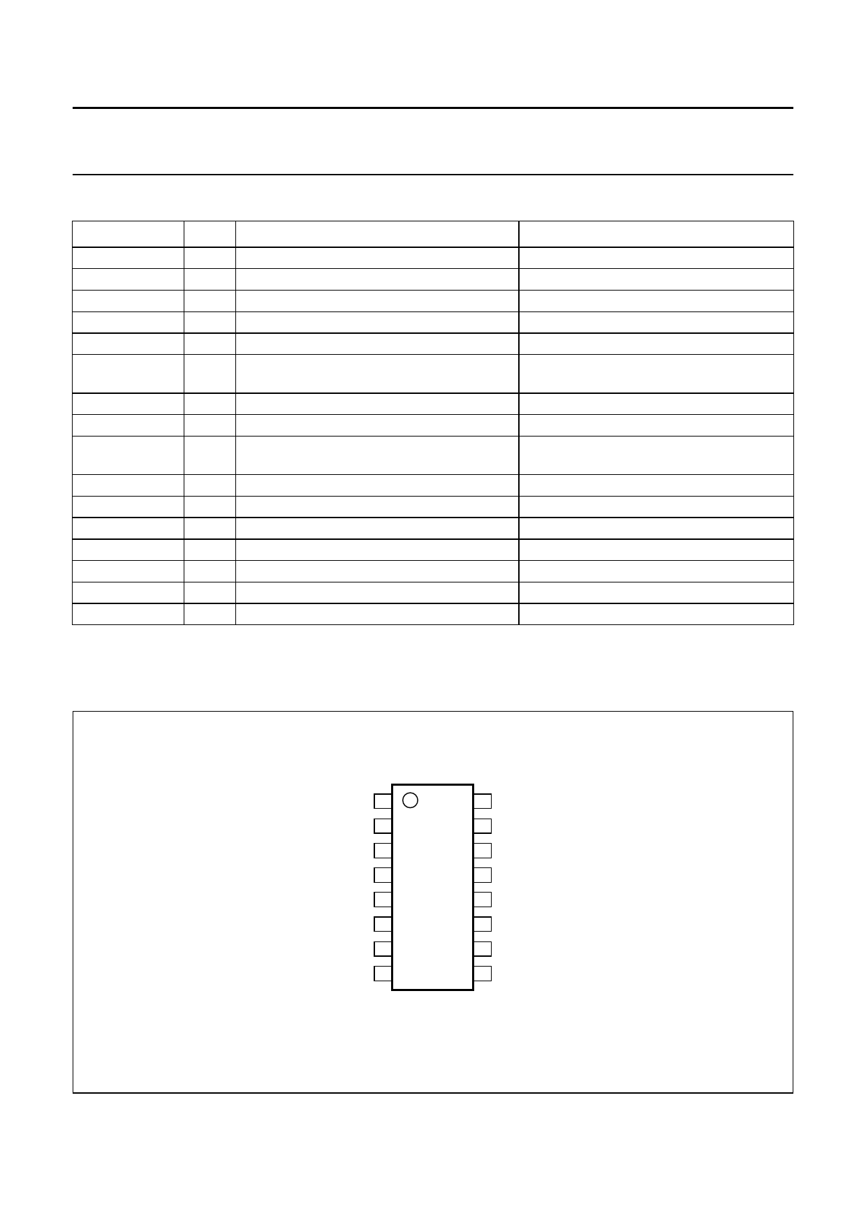
7 PINNING
SYMBOL
BCK
WS
DATAI
VDDD
VSSD
SYSCLK/PLL1
PIN
PAD TYPE
1 5 V tolerant digital input pad
2 5 V tolerant digital input pad
3 5 V tolerant digital input pad
4 digital supply pad
5 digital ground pad
6 5 V tolerant digital input pad
SFOR1
7 5 V tolerant digital input pad
MUTE
8 5 V tolerant digital input pad
DEEM/CLKOUT 9 5 V tolerant digital input/output pad
PLL0
SFOR0
Vref(DAC)
VDDA
VOUTL
VSSA
VOUTR
10 3-level input pad; note 1
11 digital input pad; note 1
12 analog pad
13 analog supply pad
14 analog output pad
15 analog ground pad
16 analog output pad
DESCRIPTION
bit clock input
word select input
serial data input
digital supply voltage
digital ground
system clock input in video mode/PLL
mode control 1 input in audio mode
serial format select 1 input
mute control input
de-emphasis control input in audio
mode/clock output in video mode
PLL mode control 0 input
serial format select 0 input
DAC reference voltage
DAC analog supply voltage
DAC output left
DAC analog ground
DAC output right
Note
1. Because of test issues these pads are not 5 V tolerant and both pads should be at power supply voltage level or at
a maximum of 0.5 V above that level.
2000 Jul 31
handbook, halfpage
BCK 1
16 VOUTR
WS 2
DATAI 3
15 VSSA
14 VOUTL
VDDD 4
13 VDDA
UDA1334ATS
VSSD 5
12 Vref(DAC)
SYSCLK/PLL1 6
11 SFOR0
SFOR1 7
10 PLL0
MUTE 8
9 DEEM/CLKOUT
MGL972
Fig.2 Pin configuration.
6
Share Link: 