NTE821 Ver la hoja de datos (PDF) - NTE Electronics
Número de pieza
componentes Descripción
Fabricante
NTE821 Datasheet PDF : 3 Pages
| |||
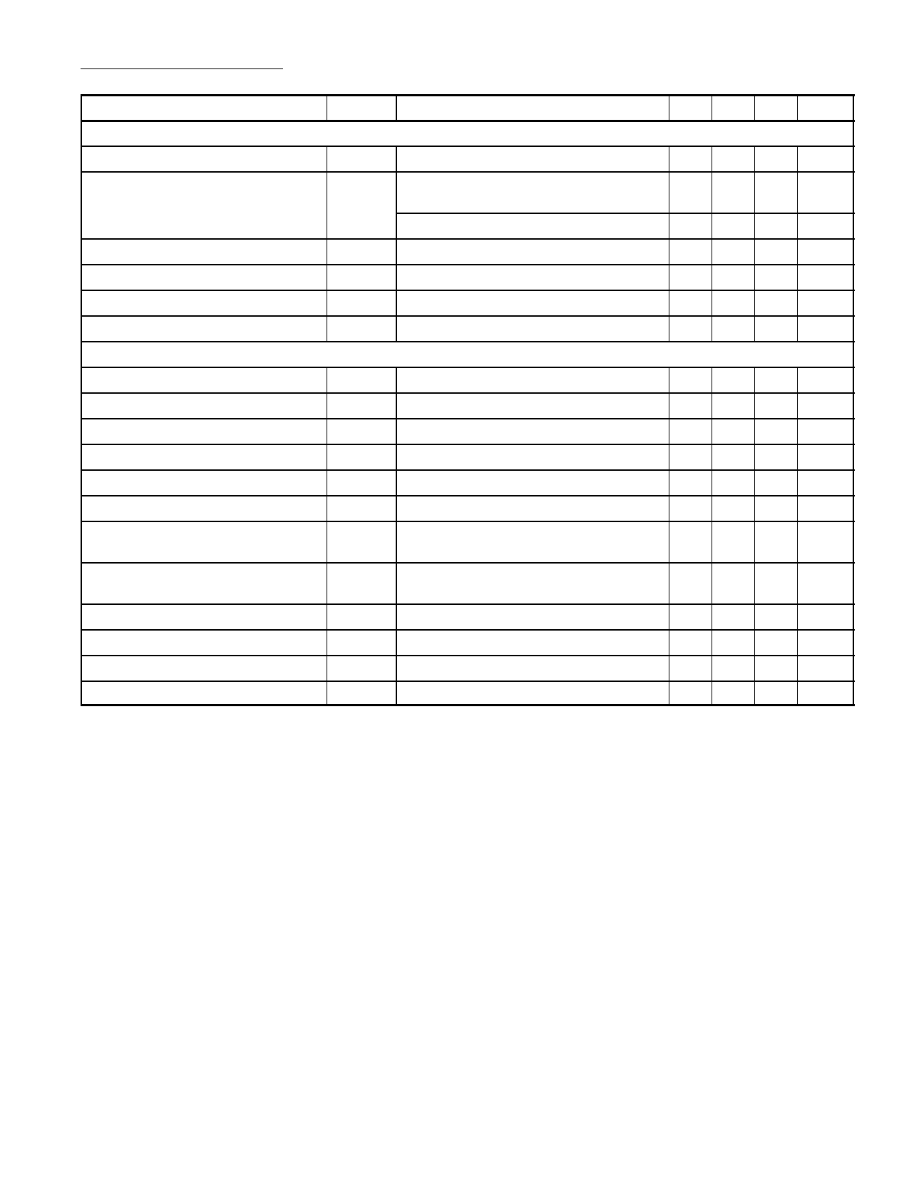
Electrical Characteristics: (TA = +25°C, VCC = 24V, RL = 3.3kΩ, Reference Input Voltage = 1VP–P
unless otherwise specified)
Parameter
Test Pin
Test Conditions
Min Typ Max Unit
Static Characteristics
Quiescent Output Voltage
9, 11, 13
13.0 14.3 16.0 V
Quiescent Input Current
8
RL = ∞, Chroma and Reference
Voltage = 0
– 6.0 – mA
Chroma and Reference Voltage = 0
16.5 19.0 25.5 mA
Reference Input Voltage
6, 7
– 6.6 –
V
Chroma Input Voltage
3, 4
– 3.5 –
V
Differential Output Voltage
9, 11, 13 Note 3
– 200 600 mV
Output Temperature Coefficient
9, 11, 13 No Output Differential Voltage, Note 3
– 2.0 – mV/°C
Dynamic Characteristics
Detector Output Voltage (B–Y)
13 Note 4
8 13 – VP–P
Chroma Input Voltage
3
B–Y Output = 5VP–P, Note 5
– 300 700 mVP–P
Detector Output Voltage (G–Y)
9
Adjust B–Y Output to 5VP–P, Note 6
1.4 1.75 2.1 VP–P
Detector Output Voltage (R–Y)
11 Adjust B–Y Output to 5VP–P, Note 6
4.3 4.65 5.0 VP–P
Relative Output Phase (B–Y to R–Y) 13–11 B–Y Output = 5VP–P
85 90 95 deg
Relative Output Phase (B–Y to G–Y) 13–9 B–Y Output = 5VP–P
236 244 252 deg
Demodulator Unbalanced Voltage 9, 11, 13 No Chroma Input Voltage and Normal – 250 500 mVP–P
Reference Signal Input Voltage
Residual Carrier and Harmonics
Reference Input Resistance
9, 11, 13 With Input Signal Voltage, Normal Refer- –
ence Signal Voltage and B–Y = 5VP–P
6, 7 Chroma Input = 0
–
– 1.5 VP–P
2.0 – kΩ
Reference Input Capacitance
6, 7 Chroma Input = 0
– 6.0 – pF
Chroma Input Resistance
3, 4
– 1.0 – kΩ
Chroma Input Capacitance
3, 4
– 2.0 – pF
Note 3. With chroma input signal voltage = 0 and normal reference input signal voltage (1VP–P), all
output voltages will be within specified limits and will not differ from each other by greater
than 0.6V.
Note 4. With normal reference input signal voltage, adjust chroma input signal voltage to 1.2VP–P.
Note 5. With normal reference input signal voltage, adjust chroma input signal voltage until the B–Y
output voltage = 5VP–P. The chroma input voltage at this point should be equal to or less than
0.7VP–P.
Note 6. With normal reference input signal voltage, adjust the chroma input signal until the B–Y out-
put voltage = 5VP–P. At this point, the R–Y and G–Y voltages will fall within the specified limits.
Share Link: 